Posted: June 05, 2017
Contributing Authors: Jeongdong Choe, Senior Technical Fellow

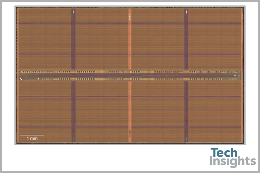
Die Photo
SK hynix successively developed their 2nd generation 21 nm DRAM technology last year. Low yield and reliability issues on 21 nm 1st generation, means their new 2nd generation 21 nm DRAM cell technology has caught the attention of many producers of memory products.
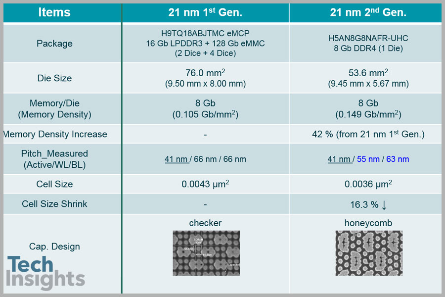
The 21 nm 2nd generation DRAM die size and memory density are quite different from the 1stgeneration. Die size has been reduced from 76.0 mm2 to 53.6 mm2 for the same 8 Gb/die, which means the memory density is increased by 42%, from 0.105 Gb/mm2 to 0.149 Gb/mm2. The active pattern pitch remains small, similar to the 41 nm, while the wordline pitch and bitline pitch are scaled down to 55 nm and 63 nm, respectively. Therefore, the cell size is reduced by 16.3 % .
SK hynix has adopted a honeycomb-type scheme instead of the checker-type for the cell capacitor. The DRAM memory density has been consistently increased to 0.056 Gb/mm2 (3x nm), 0.081 Gb/mm2 (2x nm), 0.105 Gb/mm2 (2y nm_1st) and 0.149 Gb/mm2 for the 2nd 2y nm.

Comparison SK hynix 21nm 1st and 2nd Generation DRAM Technology
From further comparison with other DRAM makers, we discovered that the SK hynix 2nd generation 21 nm DRAM has higher memory density than the Samsung 20 nm and Micron 20 nm DRAM products. For example, Samsung 2y (20 nm) DRAM has 0.142 Gb/mm2, and Micron 20 nm DRAM has 0.094 Gb/mm2, respectively.
We estimate the capacitance of the DRAM cell with 10 ~ 12 fF/cell. More details can be found in our ACE report on SK hynix 21 nm 2nd gen. DRAM (Report ID: ACE-1703-801).
As Samsung has already revealed their 1x nm (18 nm) DRAM products for DDR4 and LPDDR4/LPDDR4X to the market, we expect SK hynix’ 18 nm DRAM technology will be in our hands very shortly.


