A First Look at Infineon’s and Industry’s First 400 V SiC MOSFET
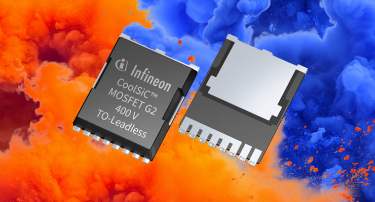
TechInsights is excited to announce that we have Infineon’s, and the industry’s, first 400 V silicon carbide (SiC) MOSFET in-house. The IMBG40R015M2H 400 V, 15 mΩ CoolSiC G2 MOSFET [1] was brought in in early September, and the initial exploratory analysis has completed.
Infineon is among the industry leaders in the semiconductor market. For the 2023 fiscal year, Infineon claimed the number 1 market share in power discrete and modules with a 20.6% figure [2]. This is also qualitatively supported in TechInsights’ Power Semiconductor Market Share 2023 Report (PWS-2407-801), where we show that Infineon leads the power semiconductor market from 2020-2023 consecutively.
To quickly rehash the SiC technology history once again, it took decades of academic research for SiC FET technology to reach first commercialization of a 1200 V JFET by now-closed SemiSouth in 2008, followed by the first 1200 V MOSFET by Cree, now Wolfspeed. The introduction of SiC MOSFETs demonstrated that the interfacial issues between the gate dielectric and the SiC material can practically be addressed. Since then, manufacturers have continually improved their device performance figures. By 2017, both Infineon and Rohm released the market’s first SiC trench MOSFETs. Furthermore, by 2024, Rohm has released its fourth-generation trench SiC MOSFET, and Infineon has released its second-generation trench SiC MOSFETs, both with significant device performance improvements over the previous generations.
Conventionally, 650 V has long been considered the practical lower limit of SiC devices with the relative cost outweighing the benefits for lower voltages. That is, until now. Voltage range below 650 V was where silicon (Si) and gallium nitride (GaN) have been the intuitive go-to for designers in terms of device selection. For this reason, Infineon’s announcement for its 400 V SiC MOSFET has garnered industrial excitement and interest. The 400 V SiC MOSFET is based on Infineon’s second generation (G2) CoolSiC technology. TechInsights released a blog on the first impression of this technology, as well as an in-depth process analysis report (PEF-2402-801) and full process flow analysis report (PFF-2404-801) on the 1200 V, 7.7 mΩ (typical) IMBG120R008M2H device.
The remainder of this blog will show the results of TechInsights’ initial analysis of the IMBG40R015M2H 400 V SiC MOSFET as well as provide commentary in the device and application contexts.
TechInsights’ First Look at the IMBG40R015M2H 400 V CoolSiC G2 MOSFET
The IMBG40R015M2H 400 V CoolSiC G2 MOSFET comes in a 7-lead TO-263 package measuring nominally 10.2 mm × 10.0 mm × 4.41 mm without leads. The package comprises a single SiC MOSFET die with the drain terminal attached to the die paddle portion of the lead frame, functioning as an external drain tab, and gate, source driver, and power source package leads are connected to the die with aluminum bond wires. The top and bottom package photographs are shown in Figure 1.
Figure 1: top (left) and bottom (right) package photographs of the IMBG40R015M2H 400 V SiC MOSFET component.
Figure 2 is a side-view package X-ray Image of the IMBG40R015M2H component. The use of Infineon’s .XT package interconnect technology [3] is evident in the minimal die-to-die paddle spacing observed in the package X-ray image. The .XT package interconnect technology replaces conventional die attach with a diffusion-based process, resulting in an ultra-thin die attach layer to offer thermal resistance improvements. This can benefit SiC MOSFETs in two ways: since SiC MOSFETs allow a higher power density than their Si counterparts, this also translates to the potential for a higher thermal concentration during operations. Improving the thermal management at the package level will be beneficial. In addition, the Young’s modulus of 4H SiC, the industry standard polytype used in SiC power devices, is about 3.1 times of that of Si’s [4]. This means a SiC MOSFET can have an elevated risk of stress and strain related delamination. The .XT technology claimed to address this compared to conventional die attach techniques to improve package reliability as well [5].
Figure 2: side view X-ray of the IMBG40R015M2H 400 V SiC MOSFET package.
Figure 3 shows the 400 V SiC MOSFET die extracted by TechInsights. From the measured die dimensions, specific-RDS(ON) figure normalized to the die area (RDS(ON)·Adie) was calculated. Compared to other SiC FETs analyzed at TechInsights, the RDS(ON)·Adie figure is about half or less of most 600-750 V MOSFETs, and comparable to the UnitedSiC (Qorvo) UJ4C075018K4S 750 V JFET, a device presented the our in-depth process report PEF-2101-801. Compared to SiC MOSFETs, SiC JFETs can inherently have a lower RDS(ON) since the gate oxide interface and channel challenges in MOSFETs are bypassed and the channel resistance component is removed from the overall RDS(ON).
Figure 3: IMBG40R015M2H 400 V SiC MOSFET die photograph.
Figure 4 shows a selected corner of the die. Initial analysis indicates a trench gate pitch of that is about a ~7% reduction from the trench gate pitch observed in the 1200 V IMBG120R008M2H previously analyzed at TechInsights (PEF-2402-801). Other sources of performance improvement, such as the MOSFET structures and substrate thickness, are yet to uncovered. TechInsights plans on performing additional analysis on the 400 V SiC MOSFET die, and the trench gate pitch measurement may further be improved in the process.
Figure 4: IMBG40R015M2H 400 V SiC MOSFET die corner photograph.
Putting the IMBG40R015M2H 400 V SiC MOSFET in Context
Table 1 is a summary of selected device parameters and calculated figures-of-merit (FOMs) based on the datasheets for the 400 V IMBG40R015M2H [1] and the 650 V IMBG65R015M2H [6] CoolSiC G2 MOSFETs. The IMBG65R015M2H was selected as a 650 V example device which also uses a 7-lead TO-263 package with a comparable 14.5 mΩ typical RDS(ON).
An inspection of Table 1 indicates that while the selected 400 V and 650 V SiC MOSFETs have comparable RDS(ON), the QGD, QOSS, EOSS, and QG values, and the related FOMs all favor the 400 V device. This indicates that to achieve the 14.5 mΩ RDS(ON) for the 650 V IMBG65R015M2H device, the die size was scaled up, leading to higher gate charge and energy loss figures. At the same time, stepping the voltage rating down to 400 V allowed design room for device and die structure optimization to fine tune these device parameters.
It may be worth noting that Infineon has also released a 400 V IGT40R070D1 CoolGaN device, also considered as a specialized voltage rating for GaN technologies. However, Infineon had stated that the 400 V SiC MOSFET is still the overall winner in designs requiring the maximum efficiency.
| Device Parameter | IMBG40R015M2H 400 V G2 CoolSiC |
IMBG65R015M2H 650 V G2 CoolSiC |
|---|---|---|
| Typical drain-source on-resistance RDS(ON) (mΩ) at 25°C and VGS = 18 V | 15 | 14.5 |
| Typical gate to drain charge QGD (nC) | 12.8 VDD = 200 V, VGS = 0-18V |
15 VDD = 400 V, VGS = 0-18V |
| Typical output charge QOSS (nC) | 101 VDS = 200 V, VGS = 0 |
148 Calculated based on COSS |
| Typical output energy EOSS (µJ) | 7.3 VDS = 200 V, VGS = 0 |
20.1 VDS = 400 V |
| Typical total gate charge QG (nC) | 62 VDD = 200 V, VGS = 0-18V |
79 VDD = 400 V, VGS = 0-18V |
| RDS(ON) × QGD (mΩ·nC) (Related to hard switching, lower is better) |
192 | 217.5 |
| RDS(ON) × QOSS (mΩ·nC) (Related to soft switching, lower is better) |
1515 | 2146 |
| RDS(ON) × EOSS (mΩ·µJ) (Related to switching efficiency, lower is better) |
109.5 | 291.5 |
| RDS(ON) × QG (mΩ·nC) (Related to gate drive power loss, lower is better) |
930 | 1145.5 |
Table 1: Selected device parameters and figures-of-merits from Infineon IMBG40R015M2H 400 V and IMBG65R015M2H 650 V CoolSiC G2 MOSFETs.
What this means in terms of applications is that in topologies where the higher voltage rating is not required, the 400 V SiC MOFET can offer better power density, switch performance, and efficiency. Such applications can include server power supplies (PSUs), inverter motor control, power supplies, as well as solar and energy stage systems. Infineon’s publication indicates the development of the 400 V SiC MOSFET was motivated by specific customer requirements and provides improved switching and conduction losses compared to the 650 V SiC MOSFETs, yielding an efficiency improvement of up to 0.3% and a flatter RDS(ON) versus temperature curve. This difference can translate to significant power difference in high-power applications, such as server power supplies (PSUs). It was stated that using the 400 V Si MOSFETs in a multi-level power factor correction (PFC), the AC/DC stage of a server PSU can reach a power density of >100 W/in³ and an efficiency of 99.5% [5] [7].
Learn more
Power semiconductor devices are essential in all electronics applications, including ever-growing markets like AI, datacenters, automotive, electric vehicles, as well as industrial and consumer electronics. TechInsights’ reports offer insights for IDMs, fabless companies, foundries, capital equipment suppliers, and product manufacturers. To see more power related information please visit the TechInsights platform.
Register for a free account and see:
- Power TechStream Blogs
- Videos
- Sample content and directory of recent power reports
- Upcoming Power Device analysis
- Upcoming PMIC Device analysis
Power Subscribers will be able to see the full Power Essentials and Process Flow early 2025.
References
- Infineon Technologies. IMBG40R015M2H Final Datasheet — CoolSiC™ 400V CoolSiC™ G2 MOSFET. 2024. https://www.infineon.com/dgdl/Infineon-IMBG40R015M2H-DataSheet-v02_00-EN.pdf?fileId=8ac78c8c8eeb092c018f5801017032f3 [accessed September 25, 2024]
- Infineon Technologies. Infineon at a glance — Fiscal year 2023. 2023. https://www.infineon.com/dgdl/Flyer_Infineon_at_a_glance_FY2023_EN.pdf?fileId=8ac78c8b8ca9ff15018ccec8fb030000 [accessed September 25, 2024]
- Infineon Technologies. .XT interconnection technology. 2024. https://www.infineon.com/cms/en/product/technology/.xt/ [accessed September 25, 2024]
- Lutz J. Packaging and Reliability of Power Modules. CIPS 2014; 8th International Conference on Integrated Power Electronics Systems, Nuremberg, Germany, 2014, pp. 1-8. https://ieeexplore.ieee.org/document/6776808 [accessed September 25, 2024]
- Daryanani S. of Infineon Technologies. Improvements in Performance and Voltage Range of SiC MOSFET. 2024. https://www.infineon.com/dgdl/Infineon-CoolSiC_G2_TechArticle-Article-v01_00-EN.pdf?fileId=8ac78c8c90530b3a0190e870d76a4e7d [accessed September 25, 2024]
- Infineon Technologies. IMBG65R015M2H MOSFET CoolSiC MOSFET 650 V G2. 2024. 2024. https://www.infineon.com/dgdl/Infineon-IMBG65R015M2H-DataSheet-v01_00-EN.pdf?fileId=8ac78c8c8d2fe47b018dd631ff3b52b3 [accessed September 25, 2024]
- Infineon Technologies. Infineon unveils CoolSiC™ MOSFETs 400 V redefining power density and efficiency in AI server power supplies. 2024. https://www.infineon.com/cms/en/about-infineon/press/market-news/2024/INFPSS202405-106.html [accessed September 25, 2024]


