Maximizing NAND Capacity per Wafer in 3D NAND Production
Navigating the Ever-Escalating Terrain of Semiconductor Innovation
In the fast-paced world of semiconductor technology, the race to maximize NAND capacity per wafer in 3D NAND production is showing no signs of slowing down. With advancements pushing the boundaries of what's possible, it's an exciting time for the industry. Let's delve into the latest trends and what they mean for the future of storage.
As of now, the maximum NAND capacity per wafer, measured at 12 inches, has surged to an impressive 128TB. This remarkable achievement is a testament to the relentless innovation driving the field forward. Figure 1 illustrates the upward trajectory of this capacity, showcasing a trend that continues to soar.
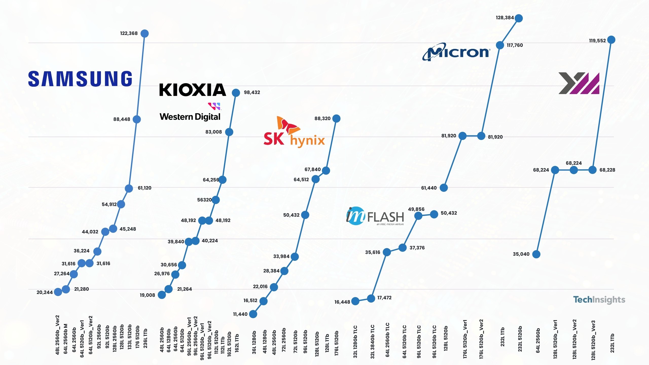
Figure 1. Max GB/Wafer (3D TLC NAND Chip Production), TechInsights Inc.
What's even more intriguing is the roadmap laid out by leading memory companies, hinting at even greater heights. With projections surpassing 800 layers, and talk of reaching the coveted 1,000-layer mark, it's clear that the ambition knows no bounds.
To achieve these lofty goals, a multi-dimensional approach is essential. Scaling not only in the X, Y, and Z directions but also increasing the number of stacks and enhancing peripheral scaling are critical steps. This holistic strategy is necessary to accommodate higher array density while maintaining performance and reliability.
Looking further ahead, the long-term vision includes innovative techniques such as wafer bonding, hybrid bonding, die stacking, and advancements in bit cell technology. These methods promise to unlock new levels of efficiency and functionality, paving the way for future breakthroughs in storage solutions.
At our recent T1 2024 NAND Analyst Briefing Seminar, we delved deep into these topics, offering insights into the 3D NAND roadmap, technology trends, comparisons, and outlook. For those who missed the seminar, fret not. You can access the slide decks and video briefing on the TechInsights Platform, ensuring you stay informed and ahead of the curve.
The pursuit of maximum NAND capacity per wafer in 3D NAND production is a journey marked by innovation, collaboration, and boundless potential. With each advancement, we inch closer to realizing the full promise of next-generation storage, transforming the way we store and access data in the digital age.