Posted: January 8, 2013
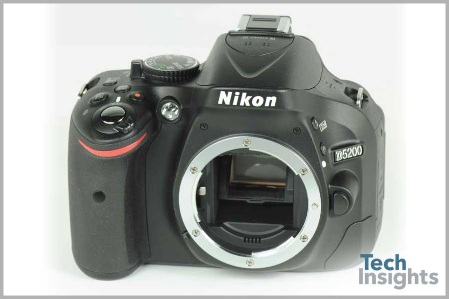
Nikon D5200 DSLR
At CES 2013 Nikon announced the US availability of a new premium-level consumer DSLR camera, the D5200.
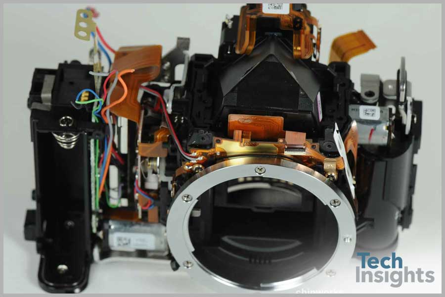
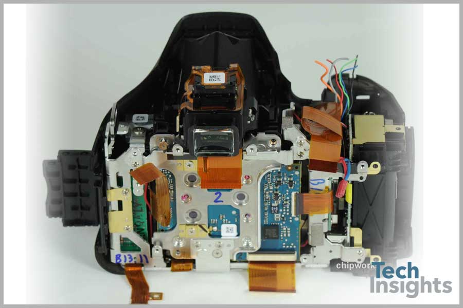
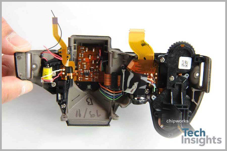
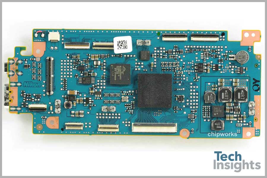
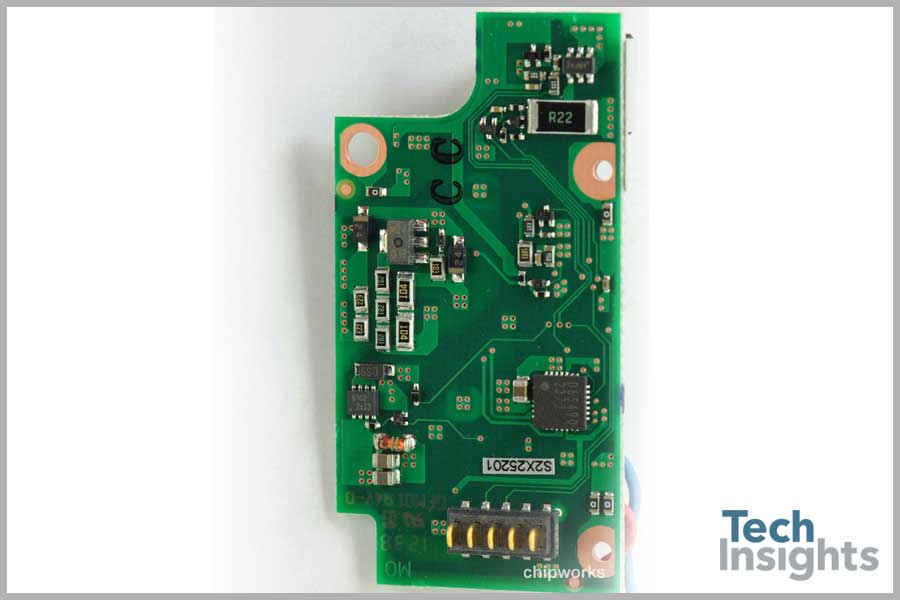
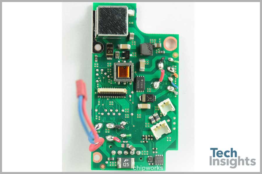
When compared to the high level of integration on a single board that one finds in a typical smart phone a DSLR is a complex system of individual parts. If you scroll through the pictures at the right, you can see why we are are amazed that they can be manufactured at all - without having large numbers of devices being RMAd.
But we digress, this teardown is about the silicon inside. First, the key features of the premium consumer-level DSLR camera:
- 24.1 MP CMOS Image Sensor
- APS-C
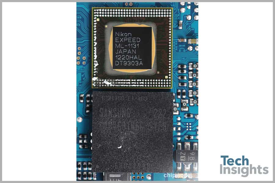
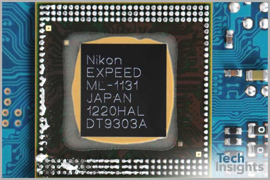
- Nikon EXPEED 3 Sensor
- 1080p at 30 fps and 5 fps burst
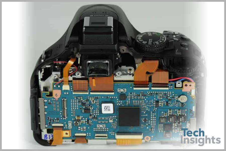
Inside Nikon D5200 DSLR
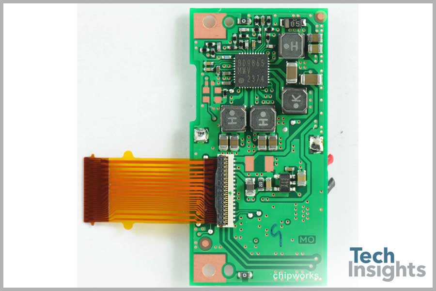
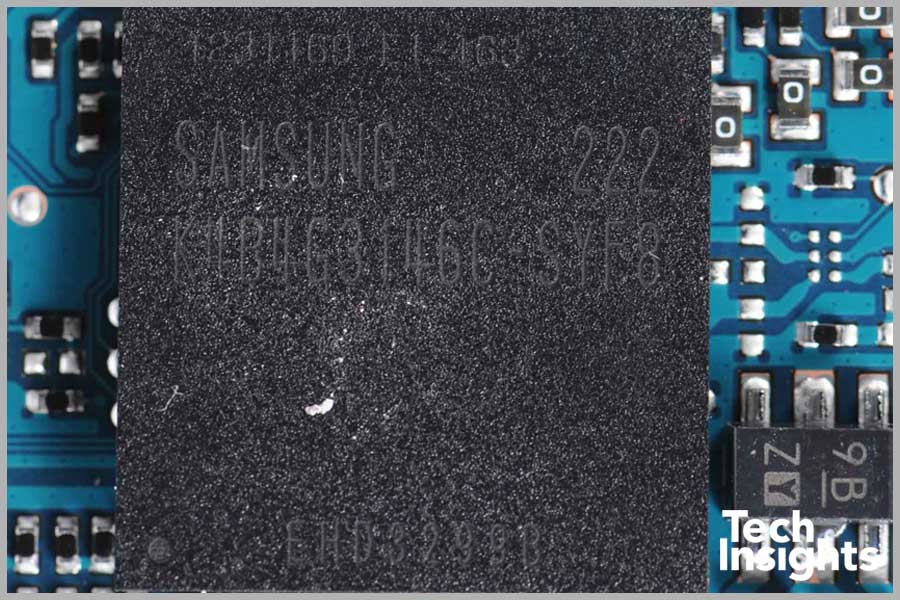
Other devices cataloged
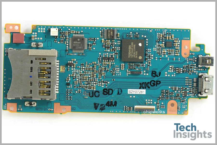
All these boards are not the most advanced, tightly packed 10-12 layer types needed in a more highly integrated handheld device and have a lot of uncatalogued passive parts. Here is the key silicon, with Rohm being a key winner:
- Toshiba TMP19A44f Microprocessor
- Wolfson WM8946E Audio Codec
- Spansion S29GL256S90D 256 Mbit NOR Flash
- Rohm Semiconductor BU9795 LCD Driver
- Rohm Semiconductor BU9798KV LCD Driver
- Rohm Semiconductor BD8965 DC-DC Regulator
- Rohm Semiconductor BD65490 Driver
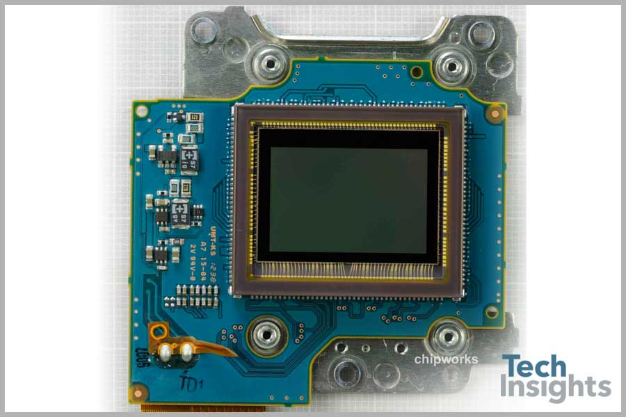
Toshiba image sensor
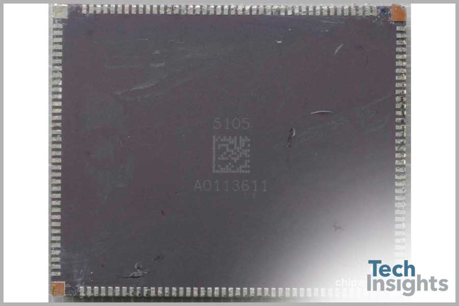
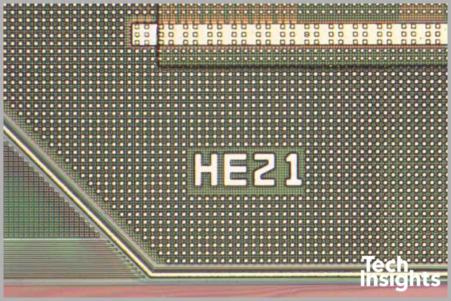
Toshiba image sensor found inside
In our recent technology blog entry on full-frame format image sensors, we speculated on the possibility of new entrants in the FF CIS space. What we didn’t expect was a new entrant into the APS-C game with Toshiba winning the primary CIS socket in the Nikon D5200.
Why is it a surprise to see Toshiba?
If you had to pick a new vendor for Nikon APS-C class sockets you would likely pick Aptina. Aptina has the design wins in the Nikon 1 system cameras (1” format V1, J1, V2), and it has previously marketed an APS-C device. The MT9H004 is a 16 Mp sensor employing Aptina’s dual conversion gain approach as part of its DR-Pix platform. The device is intended for use in APS-C class DSLR and MILC applications, but we haven’t seen a design win for it yet. Due to the existing relationship between Aptina and Nikon, you would expect that the 24.1 Mp sensor for the D5200 would have been developed by Aptina.
Toshiba has publicly announced its strategy to aggressively pursue the mobile imaging space, with a target of 30% market share by 2015. So we know it is backing image sensor technology within its semiconductor group. However, it has not broadly promoted interest in the APS-C space, and we were pleasantly surprised to see this disruptive event. We’ve typically found Nikon to use either its own APS-C designs (devices fab’d by Renesas) or Sony sensors. Adding Toshiba in to the mix makes for quite the assortment of silicon vendors used by Nikon.
Finally, our preliminary analysis shows another twist to the picture in that Toshiba are using an advanced Cu fab to manufacture the new device. This is still a rarity, as we’ve only ever seen Samsung commit a Cu fab to APS-C. We expect that an increase in DSLR and MILC resolution will drive others there eventually. Time will tell what the camera review sites have to say about the D5200s performance, but until then congratulations to Toshiba.
| Company | # of Pixel Metals | Pixel Metallization |
|---|---|---|
| Canon | 3 | Al |
| Foveon | 4 | Al |
| Nikon | 3 | Al |
| Samsung | 3 | Cu |
| Sony | 3 | Al |
| Toshiba | 4 | Cu |


