4-Part Blog Series: The state of the art of smartphone imagers
Part 3: Back-Illuminated Active Si Thickness, Deep Trench Isolation (DTI)
Posted: July 23, 2019
Contributing Author: Ray Fontaine
Content adapted from TechInsights’ paper for the International Image Sensors Workshop (IISW) 2019
Blog outline of the talk was structured in four parts:
(1) chip-stacking and chip-to-chip interconnect,
(2) pixel scaling and scaling enablers,
(3) active Si thickness and deep trench isolation (DTI) structures, and
(4) non-Bayer color filter arrays, and phase detection autofocus (PDAF).
In Part 2 of this blog series we identified DTI as a critical small pixel scaling enabler, but why? Why is DTI so important for small pixel performance?
Figure 1 illustrates the major challenges in scaling back-illuminated pixels, which include maintaining acceptable photodiode full well capacity (FWC) and suppressing crosstalk. The FWC issue is solvable through increasing the active Si thickness; however, without high performance DTI structures in place, the crosstalk issue would be a limiting factor.
Conceptually, the DTI structures are easy to understand. These can either be implemented early in the process flow from the front (front DTI, or F-DTI), or much later in the flow after the active Si thinning process (back DTI, or B-DTI). Both strategies are in high-volume production today, and both required careful development to mitigate dark current issues arising from the DTI etch process.
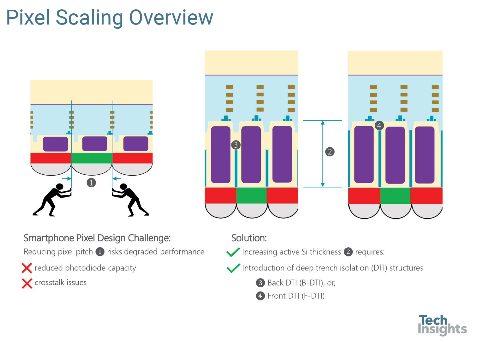
Figure 1: Small Pixel Scaling, DTI Structures
The State-of-the-Art of Smartphone Imagers
Download our paper and slides from TechInsights' presentation at IISW 2019.
Figure 2 presents a survey of selected flagship smartphone imager pixels’ active Si thickness by pixel generation. Our reverse engineering content meticulously documents the F-DTI/B-DTI evolution by IDM/foundry, but for the purposes of this blog the data set has been simplified to show the high-level trend.
DTI was first introduced to back-illuminated pixels with conventional or slightly thicker active Si, and then optimized to enable substantially thicker active Si over time. For example, DTI came to early 1.0 µm pixels with a 2.5 µm to 2.7 µm active Si thickness and later enabled active Si up to 3.9 µm thick. Studying the 0.8 µm and 0.9 µm pixel generations it is clear an active Si thickness of >3.5 µm was selected to achieve sufficient pixel performance. Another strategy we have documented is the deployment of these newer DTI structures in older pixel designs. In fact, Apples’ recent iPhone imager not only reversed the iPhone pixel scaling trend from 1.22 µm back up to 1.4 µm but simultaneously increased the active Si thickness which was enabled by B-DTI structures.
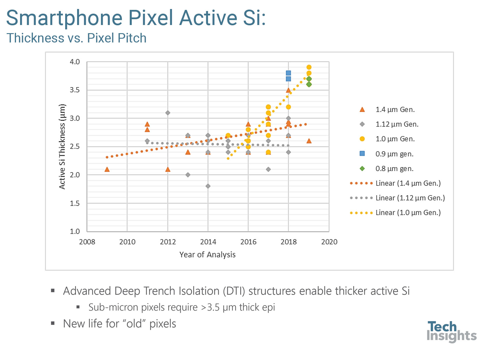
Figure 2: Back-Illuminated Active Si Thickness Trend
Recent 0.8 µm generation pixels from Sony and Samsung are shown in Figure 3, along with overviews of the DTI structures. For these specific chips Sony prefers 150 nm wide, oxide-filled B-DTI structures while Samsung prefers 110 nm wide, poly-filled F-DTI structures.
Sony’s DTI solution is implemented late in the process flow and facilitates a continuation of its planar pixel transistor strategy. Samsung’s F-DTI structures force the implementation of vertical transfer gates (VTG), but the solution results in fully isolated Si islands. We learned at the Workshop (Paper R02) that OmniVision’s 0.8 µm pixel will employ B-DTI and VTG structures.

Figure 3: DTI in 0.8 µm Generation Pixels
In the final post of this blog series we will present the topics of non-Bayer color filter arrays, and the three types of phase detection autofocus (PDAF) pixels.
The Trusted Technical Intelligence Provider
TechInsights has been at the forefront of image sensor competitive technical intelligence since 2006, and have always been the first to report on key technology elements. All Top 10 image sensor design companies are our subscribers, and all Top 3 image sensor foundries are our subscribers.