Posted: April 9, 2018
Contributing Author: Ray Fontaine
Our lab team has made good progress on structural analyses of the camera chips from Galaxy S9/S9+. While most of the details are reserved for our subscribers, we did want to share an overview as a follow up to our teardown blog. We confirmed Samsung has again dual-sourced the rear-camera chips and we expect to see the S5K2L3 (Samsung) and IMX345 (Sony) again this fall in the next-generation Samsung Note.
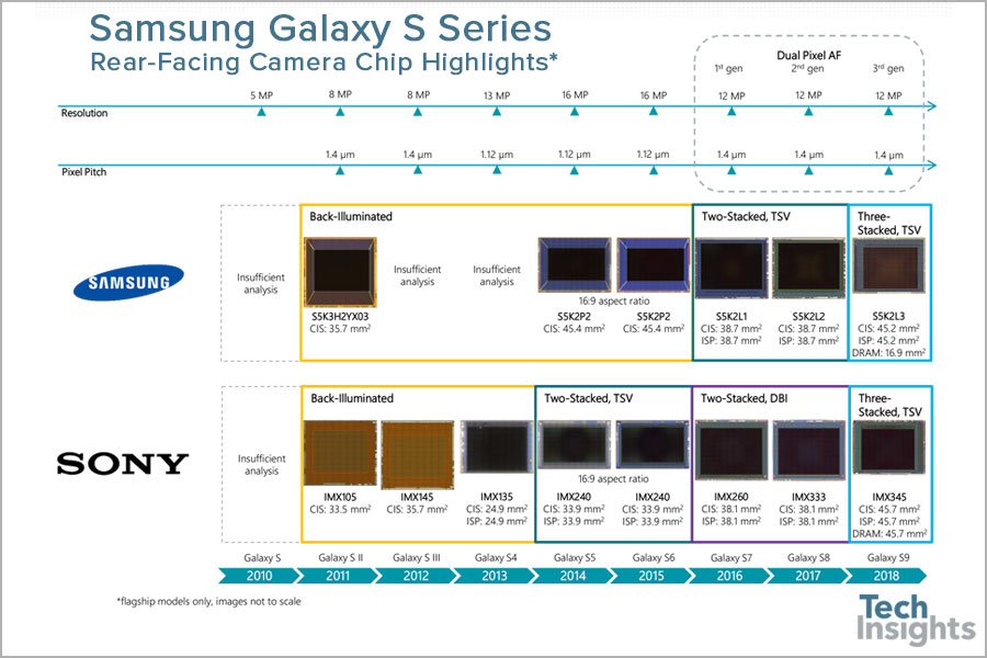
We have been tracking the emergence of multiple disruptive technology elements in the Galaxy S series’ cameras. Figure 1 summarizes a few of those findings, the latest highlight being 3-layer stacked imagers comprising a CMOS image sensor (CIS), image signal processor (ISP) and DRAM. As shown, the Samsung and Sony teams have been introducing its respective two-layer (CIS+ISP) stacking solutions at a different pace. In 2014 Sony transitioned from a conventional back-illuminated configuration to a two-layer stacked imager with through silicon via (TSV) chip-to-chip interconnect. Samsung followed two years later with its own TSV-based two-stack. At that time, Sony again leapt ahead with a Cu-Cu direct bond interconnect (DBI) solution licensed from Ziptronix (Invensas/Xperi). Finally, in 2018, both vendors have synchronized the introduction of 3-layer stacked chips, albeit implemented with substantially different fabrication techniques.

Figure 1: Selected Feature Summary of Galaxy S Series Rear-Facing Camera Chips
Sony IMX345 from Galaxy S9
The IMX345 general structure is similar to the IMX400, the world’s first 3-layer stacked imager from the year-old Sony Xperia XZs. Our initial IMX345 findings reveal Sony’s preference to continue using its first generation 3-layer stacking strategy. Wafer-to-wafer bonding and a TSV-based interconnect flow was implemented first for the DRAM and ISP wafers, and later for the CIS to thinned DRAM wafers. Note that in the IMX400, and we expect in the IMX345, the DRAM is a custom solution containing memory arrays and CIS row control circuits.

Figure 2: Sony IMX345 Package Cross-Section – Optical
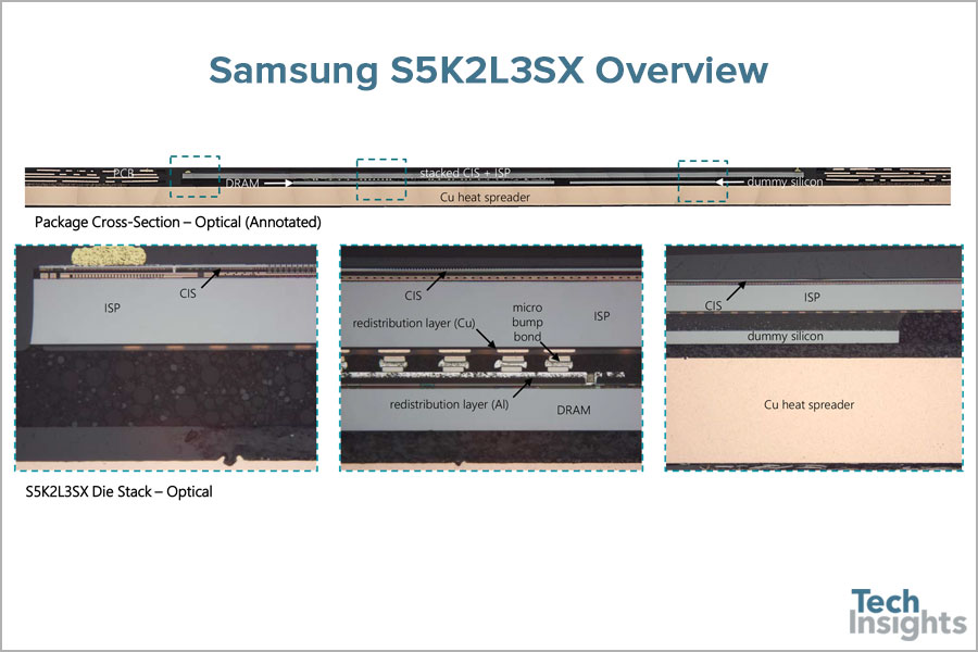
Samsung LPDDR4 DRAM from S5K2L3 Stacked Imager
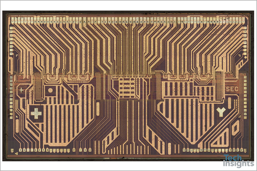
Figure 4 shows the Samsung LPDDR4 DRAM die photo with the RDL intact. The RDL routes the bump lands to the die bond pads located along the DRAM spine. The die size is 3.17 mm x 5.33 mm (16.9 mm2).

Figure 4: Samsung LPDDR4 DRAM from S5K2L3 ISOCELL Fast Imager
It is always exciting for us to analyze differences between the Samsung and Sony twins in Galaxy phones. Our latest Device Essentials reports will be available soon (S5K2L3: DEF-1803-803, IMX345: DEF-1803-804) and we’re also nearly finished with our report on the new iris scanner from Galaxy S9 (S5K5F1: DEF-1803-802).


