Advanced Packaging and Chiplets
Unleashing Semiconductor Innovation
Dive into the forefront of chiplet and advanced packaging innovation with TechInsights’ expert analysis and industry insights.
In an era where technological complexity is a staple, the semiconductor industry is continually pressed to surpass power, performance, and scalability limitations. Advanced Packaging and Chiplets are key aspects of tech giants and nation-states' relative competitive and economic advantages.
At TechInsights, we have been closely tracking these developments, equipping leaders across government, IDM, foundry, fabless, and capital equipment sectors with insights that drive informed decision-making.
Unlocking Semiconductor Breakthroughs
Explore Our New Content Series
We have launched a content series dedicated to demystifying these technologies. The series includes insights for the C-suite, in-depth market and technical analyses, and considerations for the sustainable manufacturing and packaging of semiconductors.
Defining Advanced Packaging
Advanced Packaging can broadly be defined as the application of advanced interconnect strategies to the component-level architecture; the purpose of Advanced Packaging is to support performance and cost advancements between the integrated circuit (IC) chipsets and electronics system domains to:
- Miniaturize.
- Increase performance.
- Increase interconnect density.
- Improve power efficiency.
- Disaggregate System-on-Chip (SoC) designs through the heterogeneous integration of chiplets and sub-components.
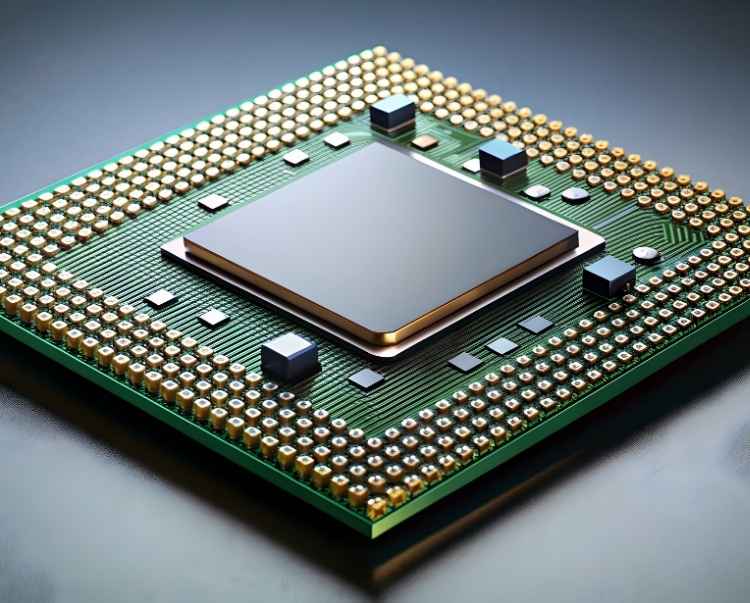
Advanced packaging themes include panel-level packaging (PLP), fan-out wafer-level packaging (FO-WLP), 2.5D with silicon/organic interposers, co-packaged optics (CPO), and 3D die stacking using through-silicon vias (TSV) or hybrid bonding with direct bond interconnect (DBI). Also included are the enabling technologies and novel packaging structures used in highly innovative imaging and sensing, mobile RF antenna-in-package (AiP), power semiconductor, and high bandwidth memory (HBM) applications.
Demystifying Chiplets: The Future of Chip Design
The world of chip design is undergoing a seismic shift with the rise of chiplet technology. But what exactly are chiplets, and why are they causing such a stir?
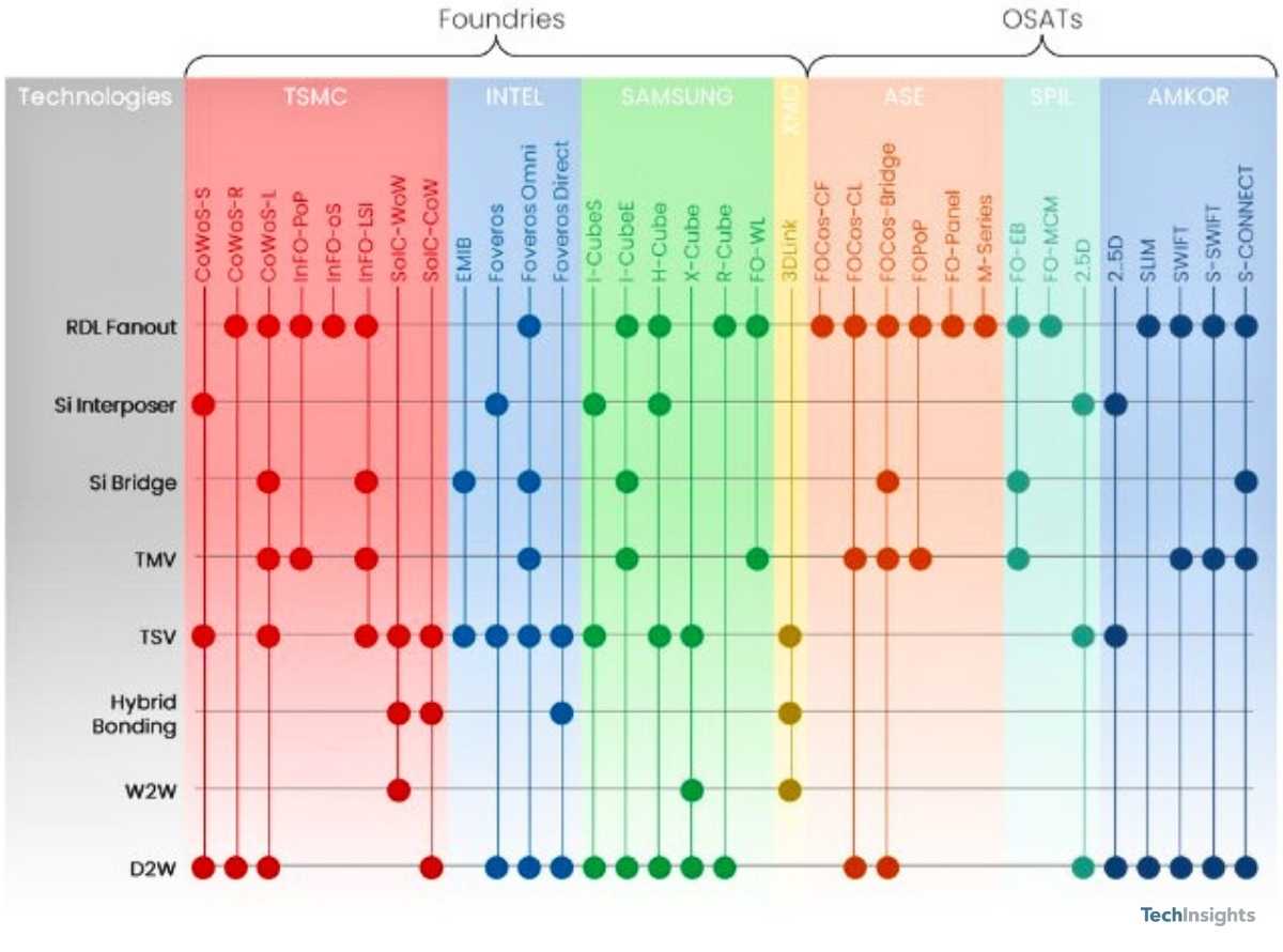
TechInsights Coverage of Advanced Packaging Technologies
Advanced semiconductor packaging is more than just a collection of technology elements. It is a strategic approach to meeting high-value applications' power, performance, area, cost (PPAC), value, and sustainability requirements. It's about differentiating conventional interconnect and packaging strategies.
TechInsights’ activities are connected through four mutually supportive focus areas:
We’re engaged 1:1 in an advisory capacity with C-suite executives, regularly discussing inflection points, company strategies, projections, historical facts, and issues between suppliers and customers. This is foundational to our own investment in Advanced Packaging as it guides contextual interpretation of industry news and market dynamics, including the effective extension of Moore’s Law. Our market summary content is the story behind the story.
The Chip Insider
Microprocessor Report
The Chip Observer
By leveraging our market understanding and analysts’ domain expertise, we generate the end market demand profiles that feed bottom-up forecasts segmented by interconnect method, substrate and package type, lead counts, chiplet type and process geometry, etc. Demand profiles feed our modeling of design starts by process generation and year, and revenue and unit shipments by the processor and chiplet type. Silicon and advanced packaging demand models then enable derivative forecasts for wafer fab equipment (WFE). This market analysis is a key input to the technical analysis target selection and product sourcing teams.
SoC Markets
Chiplets
Advanced Packaging Demand Forecast
Advanced Packaging Equipment Forecast
The value of TechInsights’ content is anchored in its privileged view of market dynamics and the synergy with technical analysis of commercialized technologies. Given the secrecy between partners in the Advanced Packaging supply chain, reverse engineering of structures, materials, and process flows is the only practical means of understanding technology insertion timelines. Analysts’ comparisons, dimensional and trends analyses, and enabling technology reviews form the basis of the TechInsights advanced packaging technology roadmap and interconnect scaling projections. The unique view into commercialized technologies provides the raw data to feed our customer’s thermal and mechanical modeling considerations and is vital input to our manufacturing simulator: a cost and price model for packaging assembly and test.
Advanced Packaging
Mobile RF IC Packaging
Image Sensor Packaging
Power Semiconductor Packaging
Manufacturing Economics, Packaging Assembly and Test Cost and Price Model
Our fact-based competitive technical intelligence products enable derivative analysis supporting sustainability initiatives that include developing processes and technologies with lower environmental impact. We’re currently modeling carbon emissions for IC and wafer manufacturing, allowing users to compare equipment, processes, and fabrication steps' environmental impact by fab site. We’re investing further to develop carbon modeling for advanced packaging, coming soon in Q3 2024.
Manufacturing Carbon Model
TechInsights Delivers Unmatched Insights into Advanced Packaging Dynamics
Designed to equip leaders with the knowledge needed to make faster, more confident business decisions, this content series explores the complexities of advanced packaging from multiple perspectives. Each installment provides deep dives into key areas shaping the semiconductor landscape.
Market Dynamics
Stay ahead with comprehensive insights into market trends and forces driving the industry.
End Market Analysis
Understand how advanced packaging solutions impact various end markets.
Chiplets
Explore the growing significance of chiplet architectures and their role in next-generation designs.
Advanced Packaging Demand Forecast
Access data-driven projections to plan for future demand.
Reverse Engineering
Gain visibility into competitor strategies through detailed teardown analyses.
Technology Roadmap
Discover how evolving technologies are shaping long-term development plans.
Process Flow
Examine the critical steps in advanced packaging manufacturing processes.
Thermal Considerations
Learn how thermal management influences packaging choices and device performance.
Test and Cost Models
Evaluate testing methodologies and cost implications to optimize production strategies.
Sustainability Carbon Model
Address environmental concerns with models designed to reduce carbon footprints.
High Bandwidth Memory
Investigate how High Bandwidth Memory (HBM) technology enhances data-intensive applications.
Hybrid Bonding
Uncover advancements in interconnect technologies improving device performance.
Co-packaged Optics (CPO)
Explore innovations integrating optical components for faster data transmission.
Antenna-in-Package (AiP)
Understand how AiP solutions are enabling compact, high-performance wireless devices.
This series delivers a 360-degree view of the advanced packaging ecosystem, ensuring decision-makers are informed, prepared, and positioned for success.
![]()
The Authoritative Information Platform to the Semiconductor Industry.

