![]()
Chiplets
Frequently Asked Questions: Chiplets and Advanced Packaging
Get ready to enter the exciting world of chiplet technology! Chiplets are tiny, specialized building blocks that are revolutionizing the way we design and build computer chips. This innovative approach is poised to unlock a new era of performance, efficiency, and flexibility. But what exactly are chiplets, and how are they changing the game? This FAQ page is your one-stop shop for all things chiplets! We'll answer your burning questions, explore the benefits of chiplet technology, and delve into how this technology is shaping the future of computing. Whether you're a tech enthusiast, a seasoned engineer, or simply curious about the latest advancements, this page will equip you with the knowledge to understand the chiplet revolution. So, dive in and discover the power of these miniature marvels!

A: Chiplets, also known as chiplets or modular dies, are individual functional blocks of a semiconductor manufactured on separate wafers. These pre-designed and pre-tested components can be interconnected using advanced packaging techniques to create a complete system.
- Increased integration: Chiplets allow for the integration of diverse technologies in a single integrated circuit. This lets designers use the optimal process for each part of a system and stitch it all together using advanced packaging, enabling more complex and powerful devices.
- Enhanced performance: By using specialized chiplets, designers can optimize performance for specific functions within a system.
- Reduced time-to-market: Utilizing pre-designed chiplets can accelerate the development process for new devices.
- Improved yield: Smaller chiplets can have higher manufacturing yields compared to larger, monolithic dies.
- Greater design flexibility: Chiplet-based design offers more modularity and customization compared to traditional SoC (System-on-Chip) approaches.
- Interconnect complexity: Chiplet integration requires high-density, high-bandwidth interconnects, which can be challenging to design and manufacture. These interconnects are often implemented as interposer or redistribution layers (RDLs).
- Testing and validation: Testing individual chiplets and ensuring proper functionality within the final device can be complex. Techniques like known-good-die (KGD) methodologies can be employed to ensure quality.
- Thermal management: Efficient heat dissipation becomes more critical as multiple chiplets are placed in close proximity within a package. Thermal management strategies include the use of heat sinks and heat spreaders.
- Standardization: The chiplet ecosystem is still evolving, and industry-wide standards for interfaces and design practices are under development. Industry and ecosystem leaders are working on creating these standards.
- 2.5D/3D integration: These techniques stack chiplets vertically using interposer layers and through-silicon vias (TSVs) for shorter interconnect distances and improved performance.
- Hybrid bonding: This bumpless technology enables ultra fine interconnect pitch and the greatest interconnect density but requires extreme planarity and alignment.
- Fan-out wafer-level packaging (FOWLP): This technique embeds redistribution layers (RDLs) within a thin wafer to create high-density interconnects for chiplets.
- Heterogeneous integration: This approach combines chiplets manufactured with different process technologies (e.g., logic, memory) within a single package.
A: Chiplets can potentially contribute to a more sustainable semiconductor industry by:
- Reducing overall die size and wafer usage, leading to lower material consumption and waste.
- Enabling the use of more energy-efficient chiplets for specific functionalities.
- Facilitating the adoption of advanced materials and processes that can improve energy efficiency.
A: Chiplets and advanced packaging are expected to be a major driver of innovation in the semiconductor industry. As technology advances, we can expect to see even greater integration, higher performance, and more diverse applications for chiplet-based designs. Future advancements may include:
- Continued development of standardized chiplet interfaces and design practices.
- Increased use of heterogeneous integration with diverse chiplet types.
- Exploration of new advanced packaging technologies like co-design and co-optimization of chiplets and substrates.
Yes, there may be. TechInsights has seen some laptop designs adopt chiplets. Examples include Intel’s Meteor Lake and AMD’s new Strix Halo. However, there are other AI developments in this space, including Qualcomm’s latest ARM based entry the Snapdragon X Elite. The Snapdragon x Elite features enough AI prowess to get Microsoft’s CoPilot+ branding, but it achieves that with integrated blocks on a monolithic die. Realistically, there are a lot of manufactures that can provision AI without using advanced packaging in this application.
If we imagine a future where the challenges around standards have all been overcome and companies are designing chiplets for an open market, there could be a significant impact. A young company could design a new product from those proven and qualified chiplets, adding perhaps only one more element of their own custom design. That could make the market more accessible. Fundamentally, it should allow Fabless companies to offload more of the design and qualification by limiting the scope of the new IC they want to produce.
Elements of these technologies have been around a long time. They have now been catapulted to the forefront because of the boom in AI and high-performance compute (HPC). Those kinds of loads require extreme bandwidth between elements, and the goal is to push optical interconnects closer and closer to the chips themselves. That looks like it going to come in steps. Shorter term, we’ll see solutions where optical is brought to the package edge, removing the losses from electrical transfer across the server board. Advanced packaging and chiplet based design are needed to allow the required integration and ability to mix process nodes.
It’s very hard to draw a line between advanced packaging and the kind of next generation processing the foundries have on their road maps. At some point, it’s just semantics and details of taxonomy. There will undoubtably be important interactions between what we consider advanced packaging today, and those future developments. However, it seems there will always be the need or desire to combine devices from different nodes or vendors, so chiplet based designs and advanced packaging will be with us for many years.
One of the key challenges for OSTAs, and even foundries now that they are so involved in packaging, is that packaging tends to be iterative. Often new packaging technologies are novel configurations or amalgamations of existing processes. That has operational knock-on effects in terms of floor space, etc. Panel-level packaging, and to a similar degree, glass core substrates, is a capital cost intensive transition. Although the same processing steps are required as for wafer-level flows, machines must be updated or replaced to handle the new format. That extends to robotic handlers and other supporting infrastructure.
The definition of chiplets is still fuzzy. Some people have a more narrow or a wider definition of what is included. You can think of them in terms of the functions of chiplet technology: CPU, analog, MCU, whatever. Or you can think of them in terms of optimizing die to the process nodes, splitting the SoC, and scalability.
The first market to really benefit from chiplet technology is in the data center. The physically larger die are becoming harder to manufacture for several different reasons. So the very complex, high-performance data center chips have been the first to be divided into chiplets. Other servers, desktop and notebook PCs have been next. TechInsights is seeing a lot of design activity and interest now in automotive. Chiplets are not yet as beneficial for smaller, space conscious applications.
It’s possible we’ll see hybrid bonding in mobile sooner rather than later. AMD V-Cache is a great example of this technology in the consumer market. AMD uses TSMC’s SoIC technology to produce the 3D V-cache parts, the same as found in their MI300 series of AI parts. In fact,hybrid bonding is already being used for the image sensors in mobile phones, as pioneered by Sony.
Laser serve lots of roles across the semiconductor industry, from production to metrology. Here are some key roles they play in advanced packaging:
- Laser dicing: 3D stacking and hybrid bonding processes are sensitive to particle contamination. One source of that contamination is chipping produced during dicing. Some flows call for plasma dicing, but others are using bulk absorptive laser dicing (e.g. Stealth Dicing).
- Wafer release layers: UV laser released temporary bonding layers are sometimes used during advanced packaging processes like handler transfer.
- Laser drilling: Laser drilling processes are commonly used in the manufacturing of the high-density organic substrates which support 2.5D and 3D packages.
Advanced Packaging
Learn how advanced packaging is revolutionizing integration, performance, and design flexibility in cutting-edge electronics. Explore the benefits, challenges, and advanced technologies like 2.5D/3D integration, hybrid bonding, and fan-out wafer-level packaging (FOWLP). Get insights into the environmental advantages and the future potential of chiplet-based designs.
Chiplets
Discover how chiplets are enabling the creation of powerful, customized devices with greater efficiency. Learn about the benefits of chiplets, from faster time-to-market to higher manufacturing yields, and explore the challenges like interconnect complexity, thermal management, and the need for industry standards.
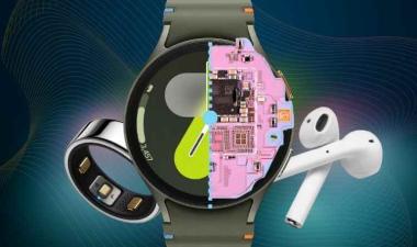
Inside the Future of Wearables | Teardown Insights & Market Trends eBook
Discover what's powering next-gen wearables. Get teardown insights, sensor trends, and strategic analysis in our free TechInsights eBook—built for tech leaders.

Huawei Matebook Fold Uses Kirin X90 Built on SMIC’s 7nm (N+2) Node
TechInsights confirms Huawei's Matebook Fold | Ultimate Design features the Kirin X90 SoC built on SMIC’s 7nm (N+2) process—debunking rumors of a breakthrough 5nm node.

Stay informed on the latest shifts in semiconductor policy, AI, packaging, and market dynamics in the June 2025 Chip Observer, featuring insights on Qualcomm, OpenAI, Huawei, and more.
![]()
The Authoritative Information Platform to the Semiconductor Industry.

