Huawei Leads Imaging Chip Area Arms Race, Sony Wins Big with i-ToF, Emergence of Event-Driven Vision Sensors
Posted: December 18, 2019
Contributing Authors: Ray Fontaine, Senior Technology Analyst
Samsung, Huawei and Apple continue to push more imaging-related silicon into their flagship smartphone cameras than ever before. In closing out the year, it is worth sharing some of our observations to complement DXOMARK’s smartphone camera benchmark scores, which reveal a continued incremental evolution of smartphone camera system performance.
Rear-Facing Flagship Smartphone Cameras
Fig. 1 shows the three-year trend of rear-facing camera resolution and pixel pitch for Samsung’s Galaxy S and Note series, Huawei’s P and Mate series, and Apple’s iPhones. Huawei continues its aggressive push to higher resolution sensors, including the dual 40 MP class sensors in the Mate 30 Pro. From a product planning perspective, it is risky business for Apple, given the small window of its annual product releases. This is contrasted by Huawei and Samsung’s twice-per-year flagship releases, where we do see more frequent introductions of new imagers and sensors. Huawei traditionally offers the most camera options across its stratified P and Mate series variants.
It is worth noting that over the past three years, none of the three leaders’ rear-facing imagers have used sub-micron pixels. Xiaomi’s new 108 MP camera features 0.8 µm generation pixels and is tied for first place with Huawei in DXOMARK’s rankings (Xiaomi data not included in Fig. 1). So, what is best? The leaders favor larger pixels in their premium products, but benchmarking aside, it does come down to a discussion of art and personal preference.
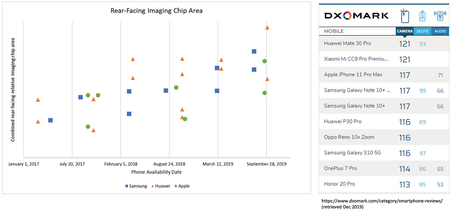
The use of higher resolution imagers, combined with the multi-camera trend, has resulted in a substantial increase in imager die size and overall stacked imager content in both rear and front-facing smartphone cameras. Fig. 2 summarizes the relative die area trend for rear-facing stacked imagers in flagship Samsung, Huawei and Apple phones (full analysis / data available in the Image Sensors subscription). Each datapoint represents the combined area of rear-facing CMOS image sensors (CIS) for each phone. These are all stacked chip imagers, so the companion image signal processor (ISP) die area is identical to the CIS die area trend. Note that the die area contribution from the DRAM IC in use in Samsung’s triple-stacked imagers is not included in this data. The strategy of each OEM is evident: Huawei is leading the imager Si arms race, while Apple has recently taken a more conservative approach, yet still achieves competitive benchmark scores.
Samsung’s recent primary rear-facing cameras continue to employ its successful triple-stacked fast readout sensor (FRS) with modest improvements to the CIS die structure. Similarly, Apple’s new rear-facing imagers feature CIS structures comparable to 2018’s iPhone, although the wide-angle camera sensor now incorporate dual PD phase detection autofocus (PDAF) complementing the incumbent masked PDAF solution. This represents the first known use of dual PD and masked PD deployed on the same active pixel array. One easily predictable trend is for small-pixel imagers to feature the increased use of specialized PDAF pixels. We have documented the emergence of masked, dual PD and 2x1 on-chip lens (OCL) approaches, but PDAF is still a relatively new pixel option and we expect more to come (e.g., Sony has just presented a 2x2 OCL paper at IEDM 2019).
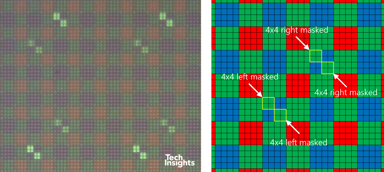
Huawei partnered with Sony and impressed with its dual 40 MP camera system in the Mate 30 Pro. Fig. 3 shows the IMX650, first used in the P30 Pro, with its 1.0 µm pixels and RYYB “Quad Bayer” color filter array (CFA). It is now paired with the new IMX608, which features the first use of a 4x4 pixels per 4.48 µm pitch CFA. This 4x4 RGB Quad Bayer configuration is the third Quad Bayer variant we have seen from Sony (the others being conventional 2x2 RGB Quad Bayer and 2x2 RYYB Quad Bayer). The IMX608’s 1.12 µm generation pixels incorporate masked PDAF. The half-masked pixels are deployed in blue-green rows with a green replacement filter used over masked pixels in the blue channel.
Fig. 3. Huawei Mate 30 Pro Rear-Facing 40 MP Camera Imagers
Smartphone Selfie Cameras
Fig. 4 shows the front-facing imager resolution and pixel pitch trends of the Top 3 OEMs. Huawei has recently employed high-resolution 24 MP and 32 MP sensors with sub-micron pixels in its selfie cameras. Samsung prefers lower resolution 10 MP selfie cameras and has recently introduced the world’s smallest dual PD PDAF at the 1.22 µm pixel generation. Apple recently upgraded its 7 MP selfie cameras to 12 MP (all have recently been using 1.0 µm generation pixels with a Bayer RGB CFA).
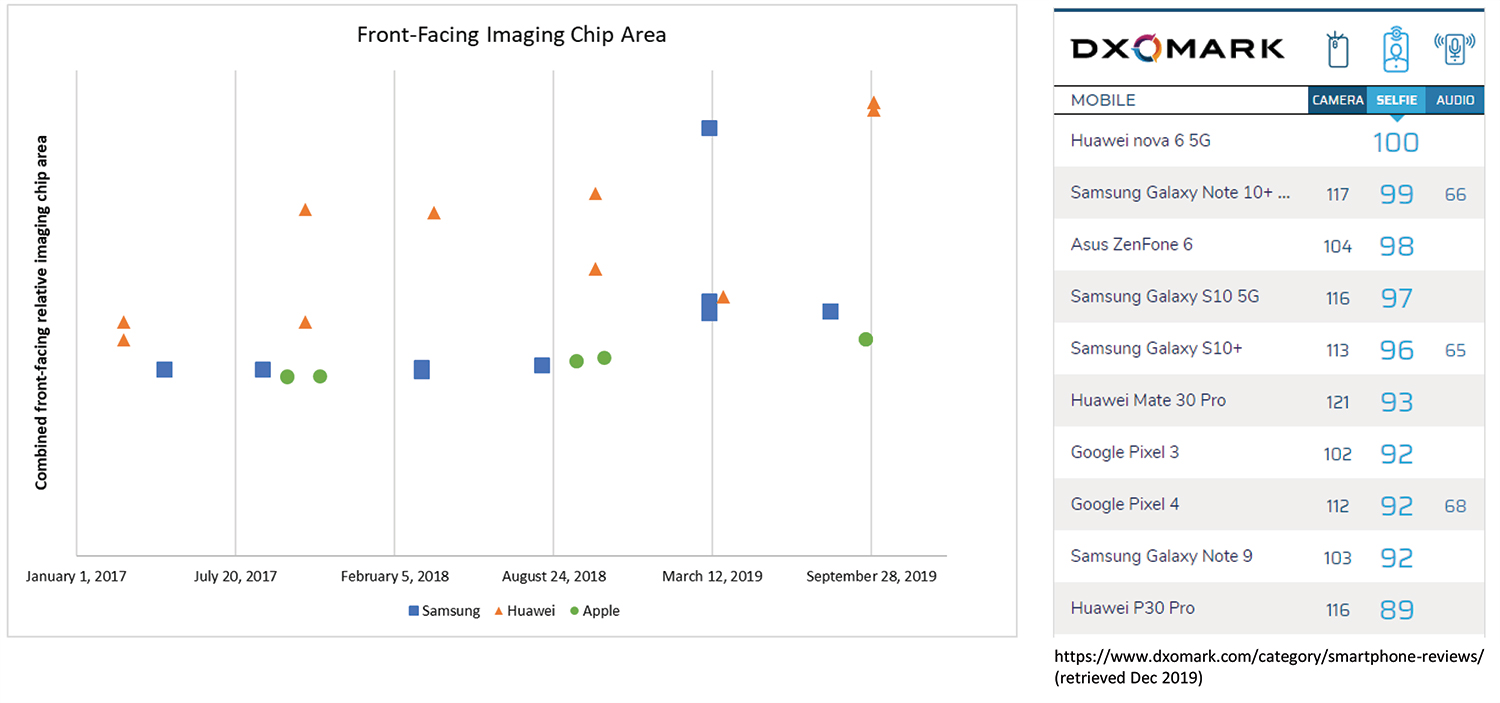
The flagship front-facing camera CIS die area trend (Fig. 5) is upward, although for Apple it is a modest increase. Samsung has recently deployed dual selfie cameras, pushing it near the top position. Huawei’s use of high-resolution Sony imagers has it leading the front-facing imager Si race, as in the rear-facing camera arena. That said, those sub-micron pixels are not buying Huawei a leadership position except when partnered with a second camera, as in the Huawei nova 6 5G (not included in the Fig. 5 die area data). Samsung is using the largest pixels in its selfie cameras and does hold the top spot amongst the top 3 OEM’s flagships.
Sony i-ToF Conquers Flagship Smartphones
Direct time-of-flight (d-ToF) has a relatively long history of use in mobile phones going back to STMicroelectronics’ original SPAD-based proximity sensors, and more recently in a competitive solution from ams. Sony’s back-illuminated indirect ToF (i-ToF) solution was first used in smartphones in 2018 and made it to Huawei and Samsung’s flagships in 2019. The emergence of array ToF is arguably the marquee smartphone imaging/sensing event of the year.
Array ToF enables new smartphone functionality, including biometrics-assist, autofocus, 3D scanning, ranging and measurement, etc. At this moment, Sony’s winning solutions offer 180 x 240 resolution with 10 µm pixels and 480 x 640 resolution with 5 µm pixels. We expect broad adoption of ToF to be realized in 2020-21, both for rear- and front-facing applications, and a continued trend of higher resolution array ToF. Sony’s success is attracting the attention of other development teams and we expect a battle for the highest resolution, smallest pixel ToF sensors over the next few years.
Fig. 6. Sony Back-Illuminated i-ToF Overview
Keep an Eye On: Event-Driven Vision Sensors
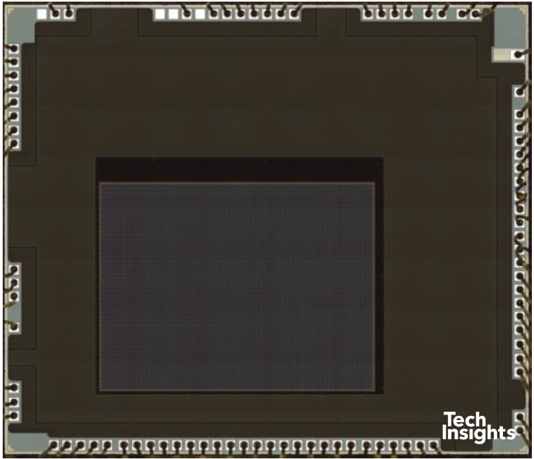
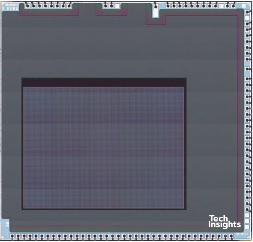
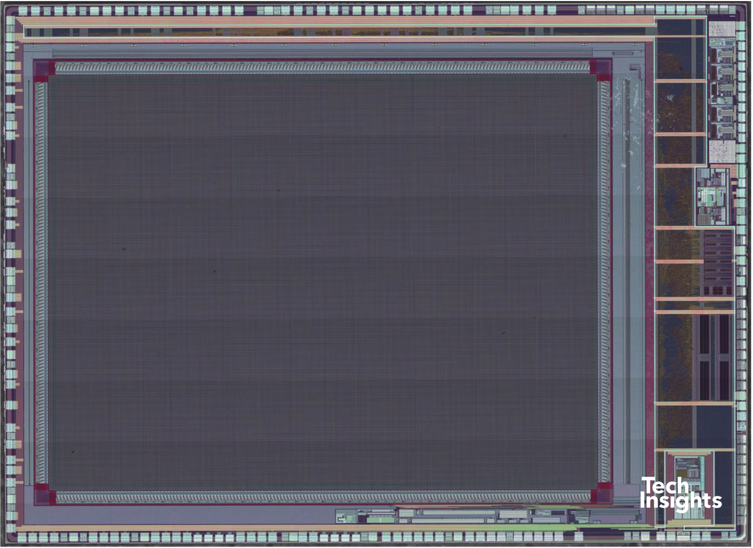
We are looking forward to our end-of-year break but are also a little bit sad to be temporarily pulled away from our in-progress analysis of Samsung’s third generation Dynamic Vision Sensor (DVS). Samsung promotes its in-home monitoring solution as offering security while maintaining user privacy. The DVS outputs a video stream showing motion/edge data instead of a traditional image stream. The back-illuminated S5K231YX has a 5.85 mm x 8.02 mm (47 mm2) die size and features a 640 x 480 resolution and 9.0 µm pixel pitch. Fig. 7 shows a polysilicon die photograph from our work in progress.
Samsung previously presented its DVS work at ISSCC 2017 and recently at IEDM 2019. We are looking forward to February at ISSCC 2020, where Sony and PROPHESEE will co-present its DVS solution (work on a back-illuminated 1280 x 720 resolution sensor will be disclosed).
2019 has been a busy year for TechInsights’ imaging and sensing specialists and analysts. The game within the game has us focused on further deep trench isolation (DTI) development, advanced small-pixel PDAF systems, evolutions in stacked chip imagers and chip-to-chip interconnect, advanced ISPs, optimized CFAs and optical stacks, high dynamic range (HDR) automotive imagers and of course ToF. We are looking forward to more back-illuminated global shutter products to analyze, continued high resolution and sub-micron pixel development, enhanced near-infrared (NIR) sensors, and the push towards non-Si detectors. As we develop our 2020 analysis roadmap, we have line of sight on several disruptive technical events and are excited to continue adding to our technical analysis content library.

The Trusted Technical Intelligence Provider
TechInsights has been at the forefront of image sensor competitive technical intelligence since 2006, and have always been the first to report on key technology elements. All Top 10 image sensor design companies are our subscribers, and all Top 3 image sensor foundries are our subscribers.


