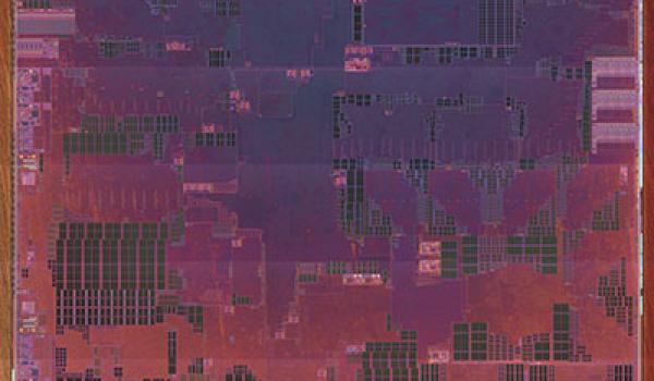
This report contains the following detailed information:
- Selected teardown photographs, package photographs, package X-rays, die markings, and die photographs
- Scanning electron microscopy (SEM) plan-view micrographs showing the layout of the die at the levels including fin/shallow trench isolation (STI), gate, contacts, and minimum pitch metals
- Measurements of horizontal dimensions of some of the major layout features, particularly the pitch and track height of standard cells
- Plan-view optical micrograph of the die delayered to the metal gate level
- Identification of major functional blocks on a gate level die photograph
- Table of functional block sizes and percentage die utilization
- High-resolution top metal and gate level die photographs delivered in the CircuitVision Software
The authoritative information platform to the semiconductor industry.
Discover why TechInsights stands as the semiconductor industry's most trusted source for actionable, in-depth intelligence.
1891 Robertson Rd #500, Nepean, ON K2H 5B7
Copyright © 2024 TechInsights Inc. All rights reserved.


