EXPERIENCE THE WEBINAR
The Samsung Galaxy S23 Ultra - Inside the Flagship
April 5, 2023
In this exclusive webinar, our experts will deliver an in-depth analysis of the components within this device, highlight what changed from previous versions, and forecast how this might impact other smartphone and parts manufacturers. Our market analysts will also share their forecasts and industry insights for Samsung and other industry leaders within the ever-competitive smartphone marketplace.
Contributing Authors: Daniel Yang, Ray Fontaine
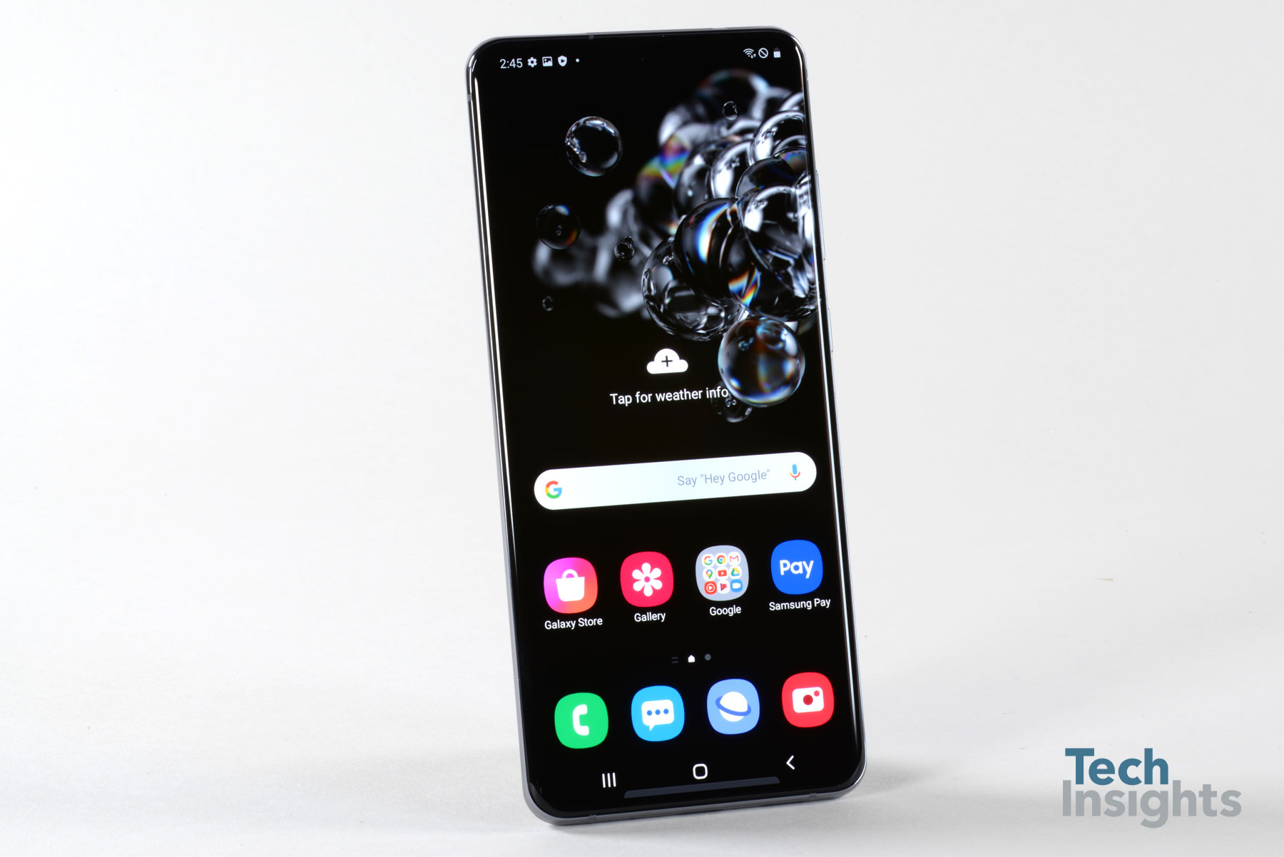
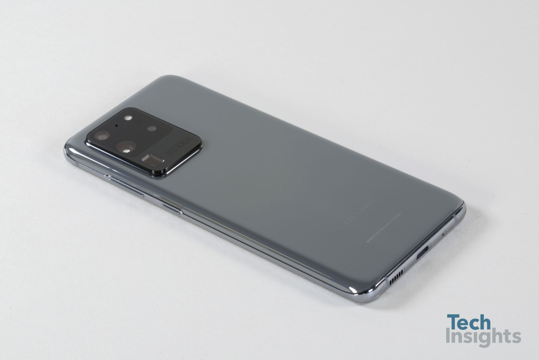
It is an especially busy time in TechInsights’ labs. Just a few days after we started the teardown of various models of the Xiaomi Mi 10 flagship series - the world’s first Qualcomm Snapdragon 865 platform phone that also supports LPDDR5 - we now have the Samsung Galaxy S20 Ultra 5G.
The model of Samsung’s key flagship that we examined for this blog is the SM-G988N, 12 GB + 256 GB, shipped to us from Korea.
Regarding cellular network bands, the SM-G988N supports 5G NR sub-6 GHz, 3.5 GHz to be exact. We also plan to examine the Samsung Galaxy S20 Ultra 5G models that support the 5G NR mmWave bands when we get those phones in our labs.
Board Images
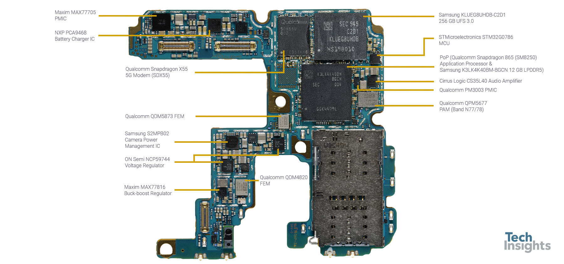
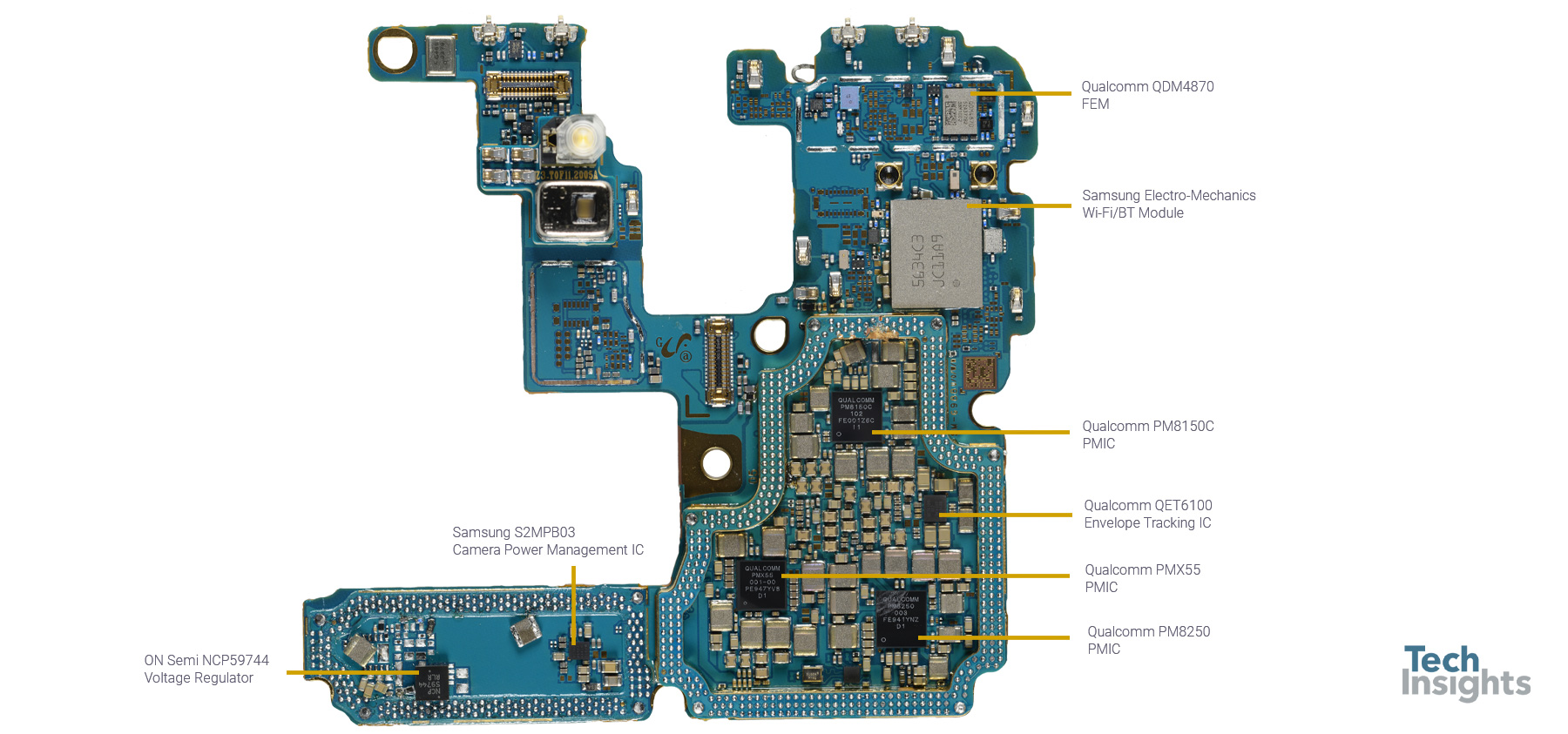
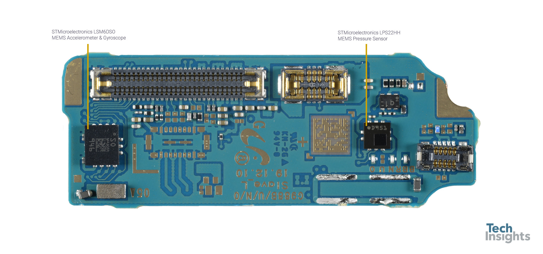
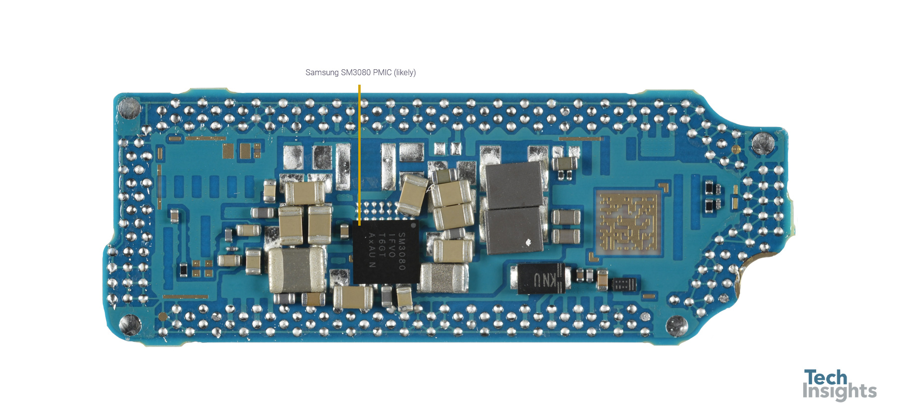
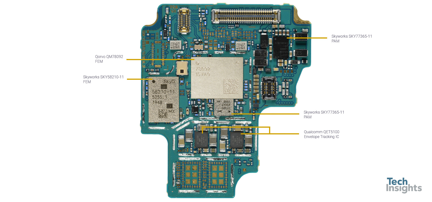
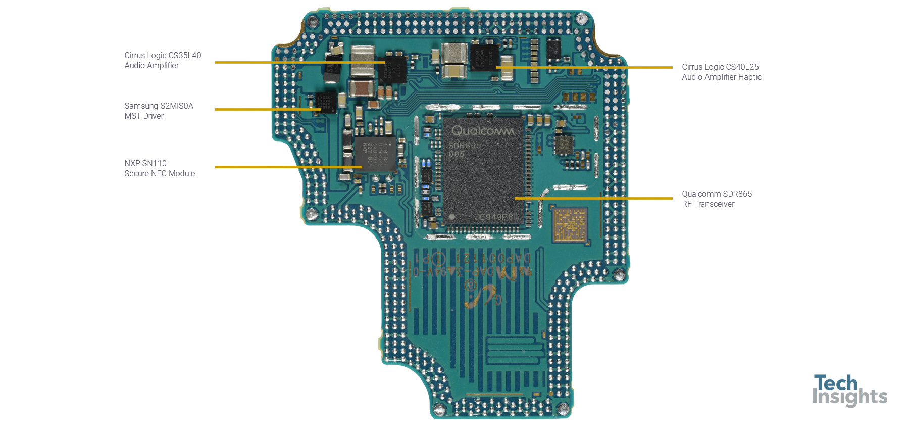
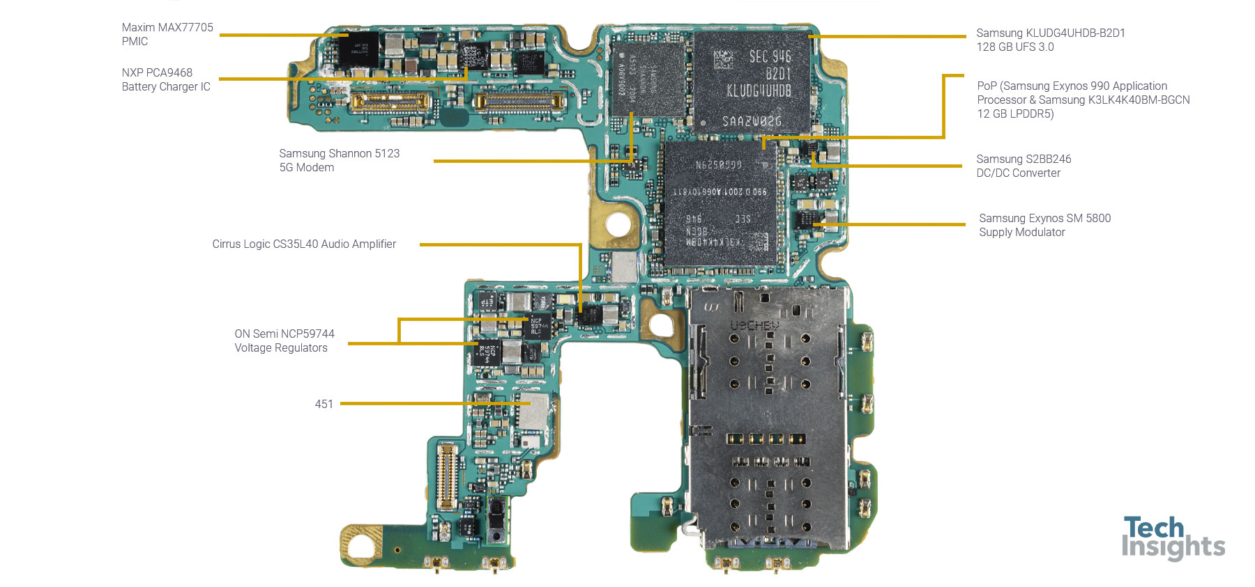
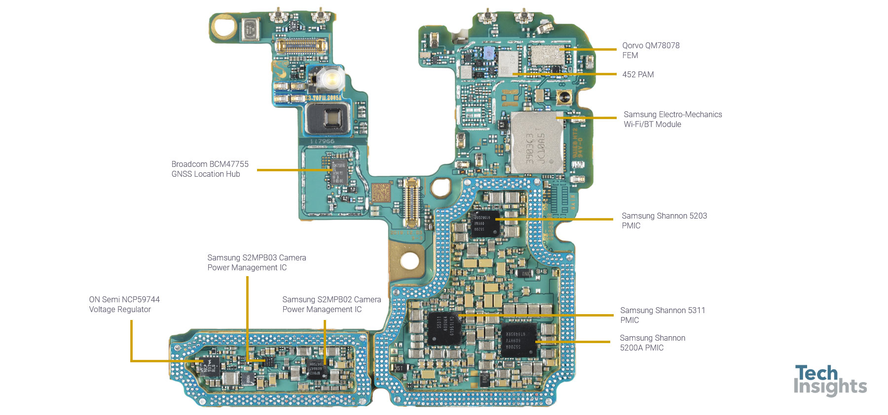
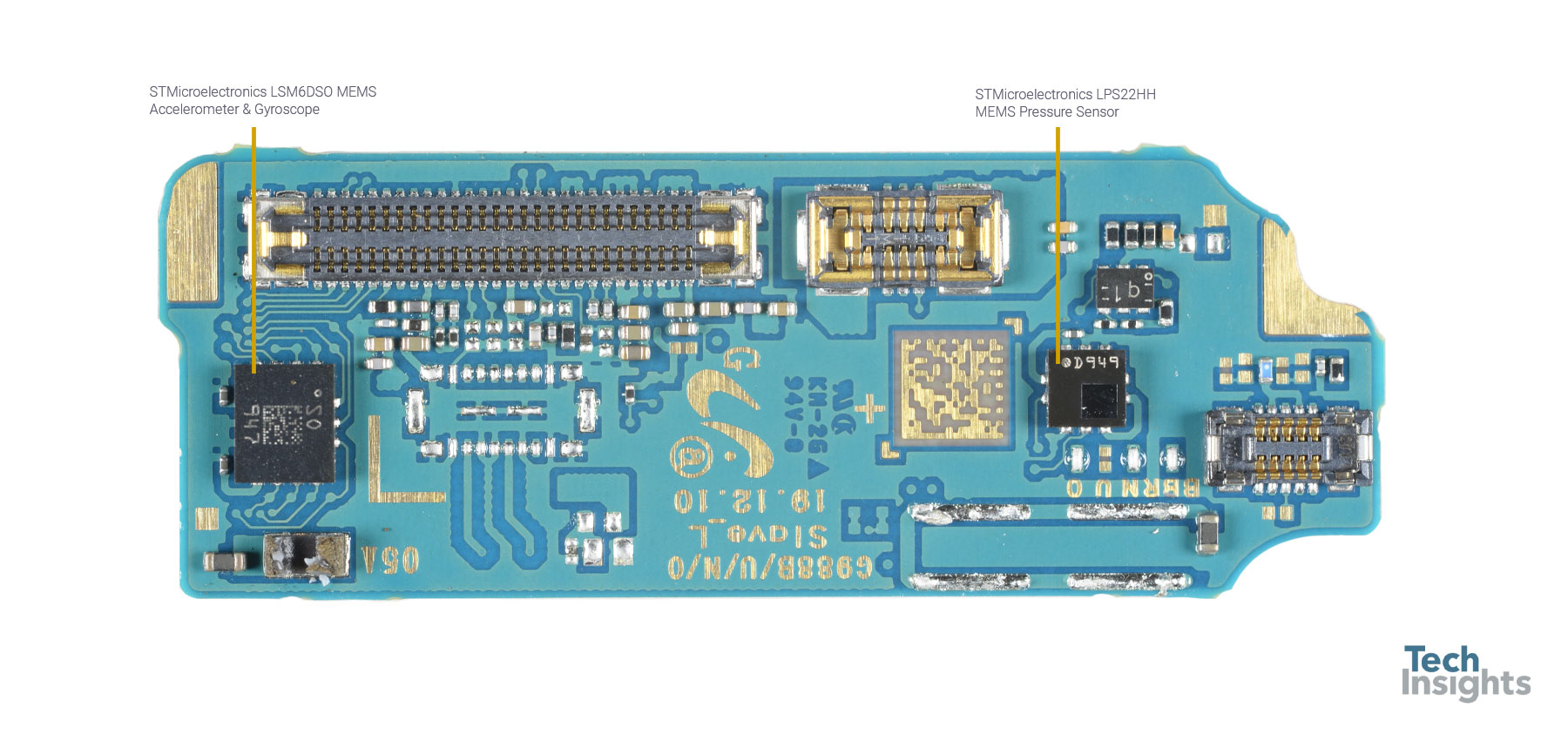
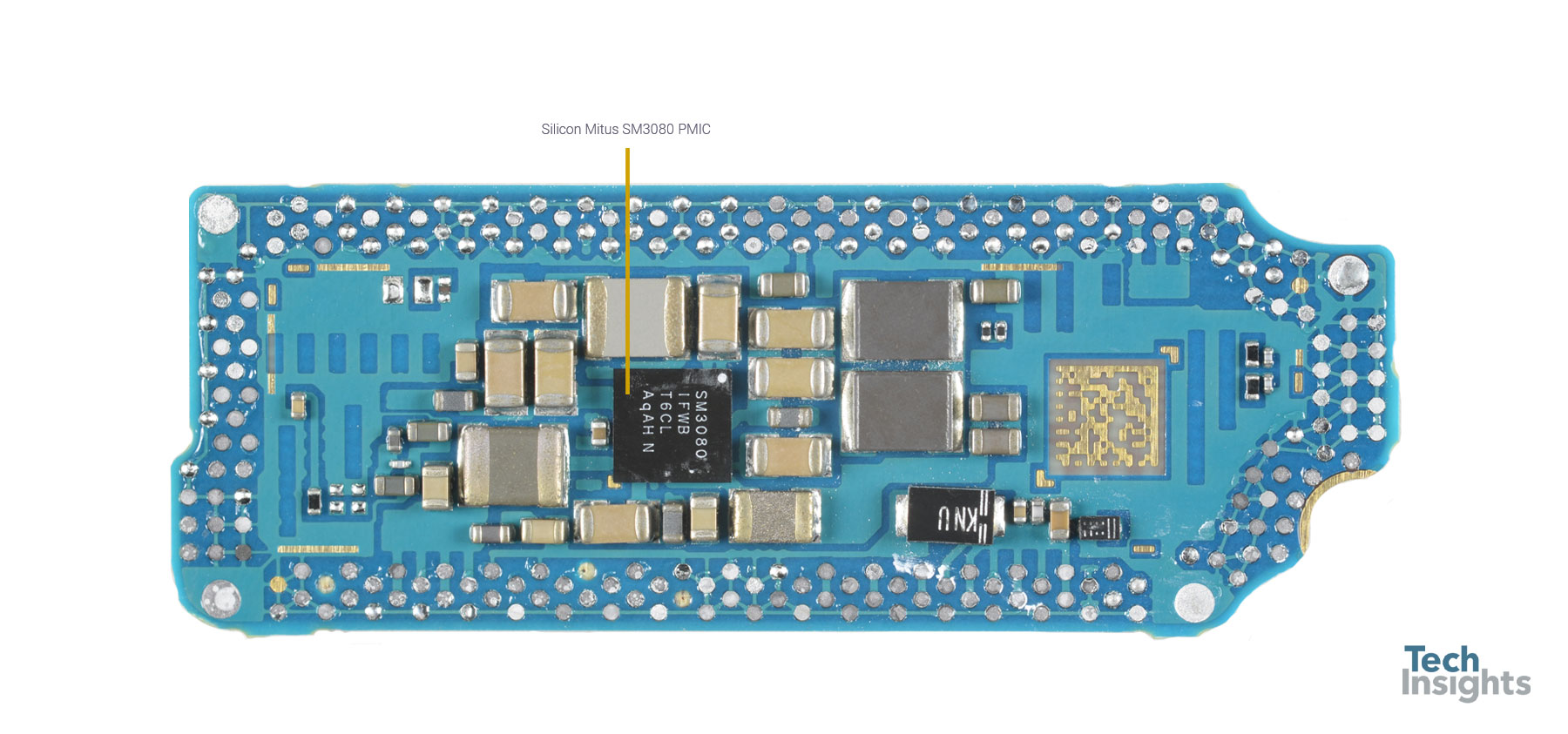
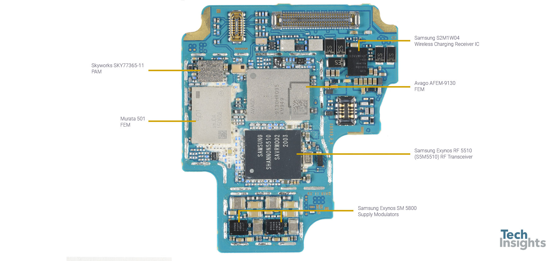
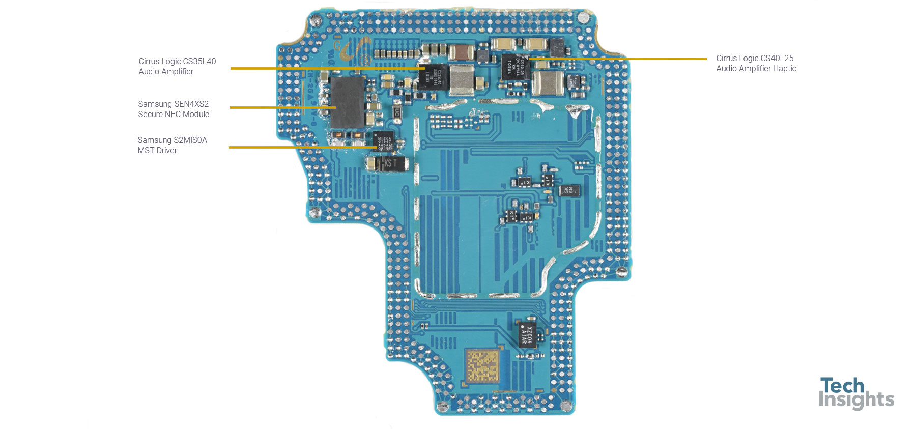
The following annotated board images show the design wins we have identified so far.
| Design Wins |
|---|
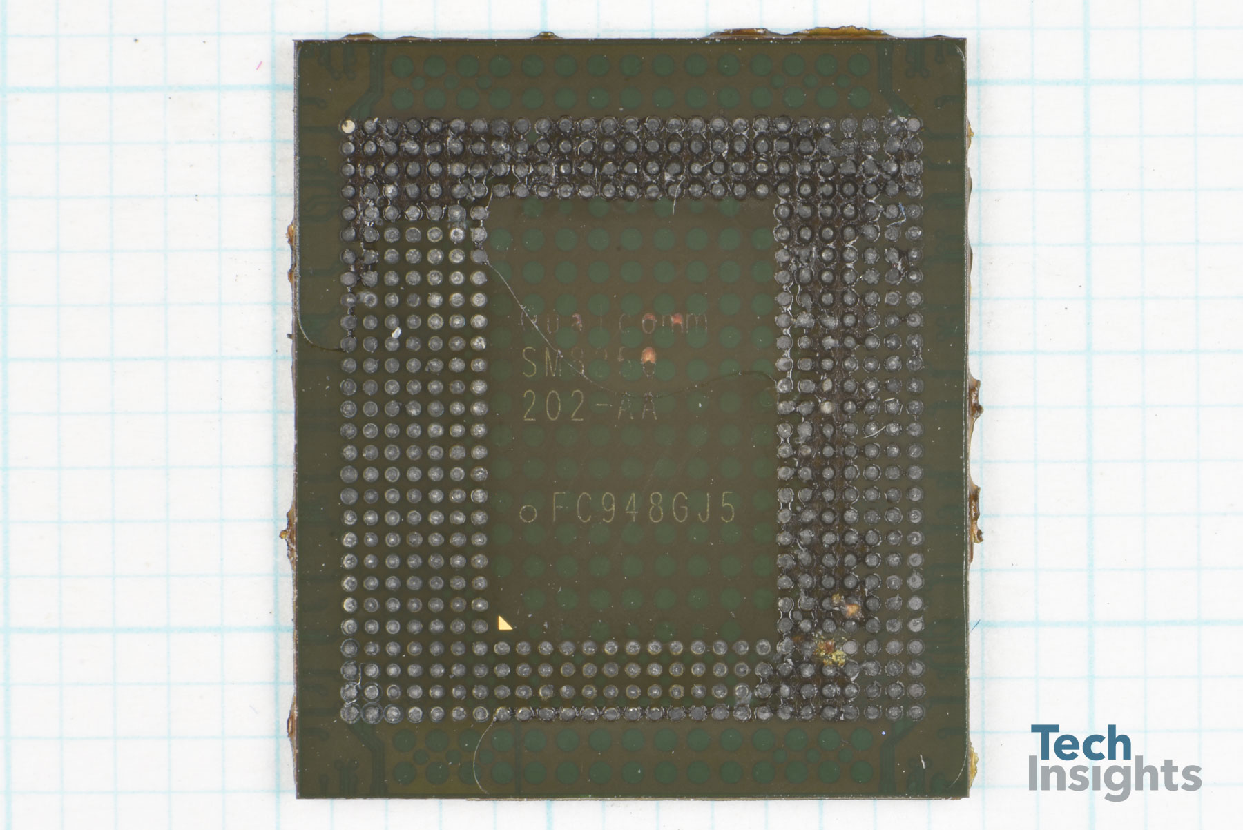
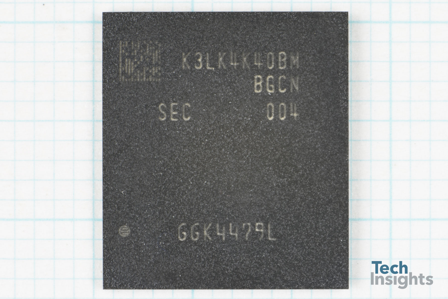
| PoP (Qualcomm Snapdragon 865 (SM8250) Application Processor & Samsung K3LK4K40BM-BGCN 12 GB LPDDR5) |
| Qualcomm Snapdragon X55 5G Modem (SDX55) |
| Samsung KLUEG8UHDB-C2D1 256 GB UFS 3.0 |
| Maxim MAX77705 PMIC |
| STMicroelectronics STM32G0786 MCU |
| Qualcomm PM3003 PMIC |
| Cirrus Logic CS35L40 Audio Amplifier |
| Qualcomm QPM5677 PAM (Band N77/78) |
| Qualcomm QDM5873 FEM |
| Samsung S2MPB02 Camera Power Management IC |
| ON Semi NCP59744 Voltage Regulator |
| Maxim MAX77816 Buck-boost Regulator |
| Qualcomm QDM4820 FEM |
| Design Wins |
|---|
| Qualcomm QDM4870 FEM |
| Samsung Electro-Mechanics Wi-Fi/BT Module |
| Qualcomm PM8150C PMIC |
| Qualcomm PMX55 PMIC |
| Qualcomm PM8250 PMIC |
| Qualcomm QET6100 Envelope Tracking IC |
| ON Semi NCP59744 Voltage Regulator |
| Samsung S2MPB03 Camera Power Management IC |
| Design Wins |
|---|
| STMicroelectronics LSM6DSO MEMS Accelerometer & Gyroscope |
| STMicroelectronics LPS22HH MEMS Pressure Sensor |
| Design Wins |
|---|
| Qorvo QM78092 FEM |
| Skyworks SKY58210-11 FEM |
| Qualcomm QET5100 Envelope Tracking IC |
| Skyworks SKY77365-11 PAM |
| Samsung S2M1W04 Wireless Charging Receiver IC |
Mobile Chipset
To our surprise, the Galaxy S20 Ultra 5G SM-G988N purchased in Korea includes the Qualcomm Snapdragon 865 platform, rather than Samsung’s own Exynos 990 platform. In recent years, Samsung has always used their own Exynos platforms in their Galaxy flagship phones in the Korean and European markets, while Qualcomm Snapdragon platforms have usually been used in Galaxy phones in the US, China, and other international markets. Here, however, Samsung has broken the trend. This is the first time in recent years that we have seen a Korean model Galaxy phone implemented on the Snapdragon platform.
The inclusion of the Qualcomm Snapdragon 865 platform means the Samsung Galaxy S20 Ultra has something else in common with the Xiaomi Mi 10, in addition to the Snapdragon 865 Application Processor SM8250, X55 5G modem, RF Transceiver SDR865, etc.
LPDDR5
The LPDDR5 is the same Samsung 12 GB K3LK4K40BM-BGCN as what we have seen in the Xiaomi Mi 10 teardown. TechInsights has a great deal of analysis planned for this part.
Image Sensors
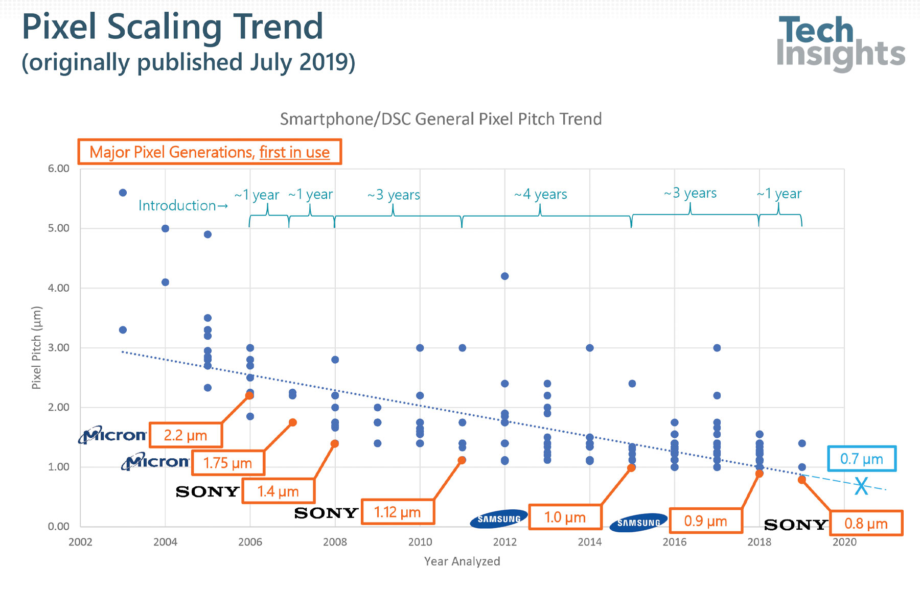
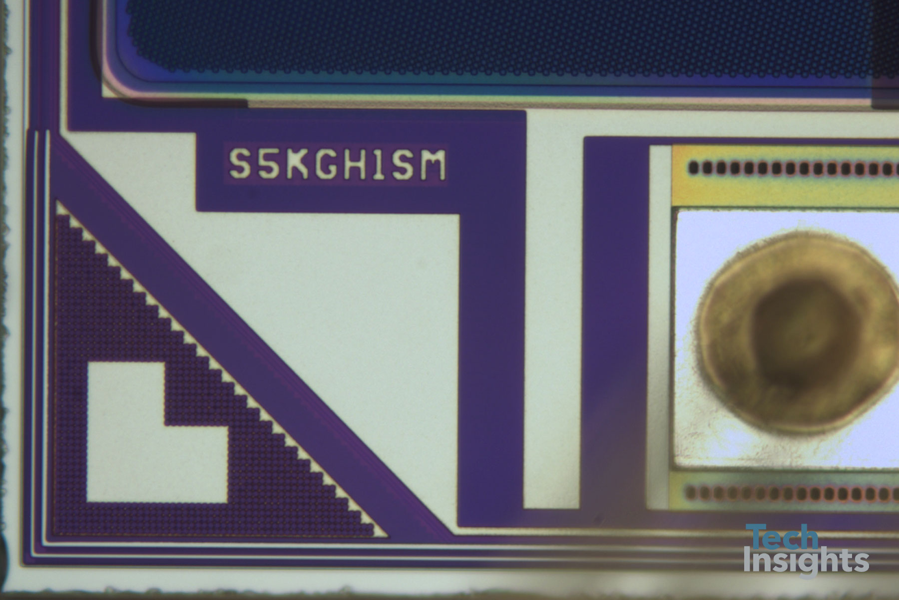
Congratulations to the Samsung team for not only delivering a well spec’d camera system, but also for being first to market with 0.7 µm generation pixels! The GH1 stacked imager, announced in September 2019, is in use in the S20 Ultra 5Gs front-facing camera. Referring to our discussion of small-pixel market availability from July 2019, the trendline on our data shows the 0.7 µm pixels in S20 Ultra 5G have arrived right on schedule. At the time we had expected it would take another few quarters to march deeper into sub-micron pixel territory, so we are happy the trendline got it right. It is not a trivial accomplishment and we are eager to dig into the GH1s enabling technology elements.
The GH1, which uses ISOCELL Plus technology, has a reported resolution of 7968 x 5840 (43.7 MP). The die we are analyzing is 5.13 mm x 6.51 mm (33.4 mm2) with an active pixel array size of 3.89 mm high by 5.63 mm wide (6.84 mm diagonal). The Tetracell color filter array is in use and manipulating the contrast on our optical images we can see an artifact of the Super-PD phase detection autofocus (PDAF) pixel pattern. We have documented Samsung using masked and 2x1 on-chip lens (OCL) PDAF on different 0.8 µm generation sensors. Here at the 0.7 µm generation we expect only 2x1 OCL PDAF will be used, as on the GH1.
One other topic to mention on this world’s first 0.7 µm pixel sensor is the stacked chip interconnect strategy. The through silicon via (TSV) arrays visible in our die photograph show us immediately that Samsung has not yet adopted a Cu-Cu direct bond interconnect strategy as we have observed in Sony and TSMC fabricated imagers.
Samsung Galaxy S20 Ultra SM-G988B/DS
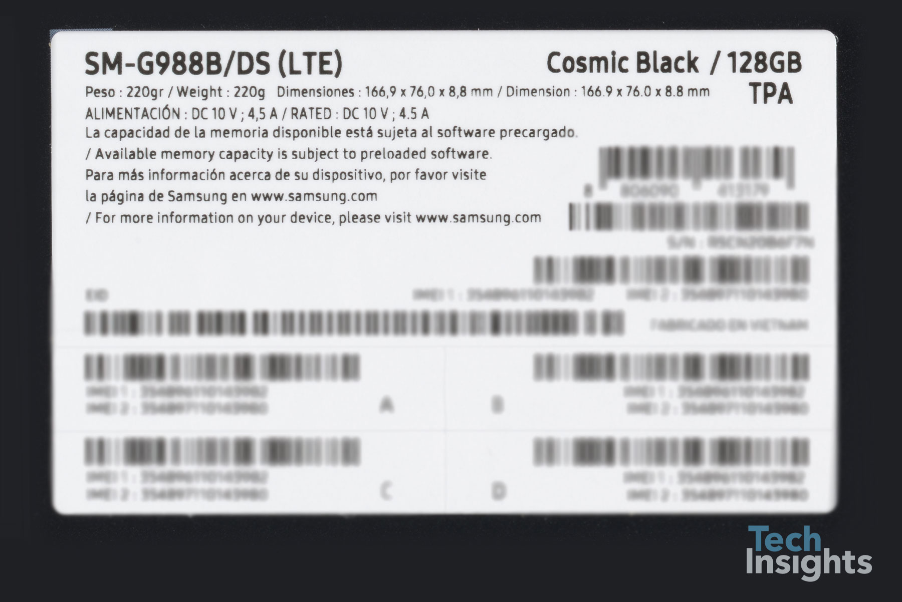
We have purchased another Samsung Galaxy S20 Ultra SM-G988B/DS, and found something else that surprised us: we thought that all Samsung’s Galaxy S20 Ultra models support 5G, but the SM-G988B/DS we have in our hands shows LTE on the box.
The teardown has shown that the SM-G988B/DS is powered by Samsung’s own mobile platform, including the Exynos 990 Application Processor, Exynos 5G modem 5123, Exynos RF 5510 RF Transceiver, and related PMICs and Envelope Tracking ICs.
To our surprise, the Galaxy S20 Ultra LTE model uses the 5G modem 5123 and the 5510 RF Transceiver. We are not yet sure of which cellular bands the Power Amplifier Module and Front-end Module serve, so we are not able to tell if the 5G PAMs and FEMs are included in this LTE model phone. We will compare the silicon contents in this Samsung Exynos-powered Galaxy S20 Ultra LTE to the same Exynos-powered Galaxy S20 Ultra 5G phone once we have it.
Similar to the Qualcomm Snapdragon 865 platform, the Samsung mobile platform adopts the Exynos 990 Application Processor. It also includes an external 5G modem 5123, which makes it different from other 5G SoC platforms we have analyzed such as the Qualcomm Snapdragon 765G, Samsung Exynos 980, HiSilicon Kirin 990 5G, or MediaTek Dimensity 1000L MT6885, where the 5G modem is integrated in the 5G SoC.
| Design Wins |
|---|
| PoP (Samsung Exynos 990 Application Processor & Samsung K3LK4K40BM-BGCN 12 GB LPDDR5) |
| Samsung Shannon 5123 5G Modem |
| Samsung KLUDG4UHDB-B2D1 128 GB UFS 3.0 |
| Maxim MAX77705 PMIC |
| NXP PCA9468 Battery Charger IC |
| Samsung S2BB246 DC/DC Converter |
| Samsung Exynos SM 5800 Supply Modulator |
| Cirrus Logic CS35L40 Audio Amplifier |
| ON Semi NCP59744 Voltage Regulators |
| 451 |
| Design Wins |
|---|
| Qorvo QM78078 FEM |
| 452 PAM |
| Samsung Electro-Mechanics Wi-Fi/BT Module |
| Samsung Shannon 5203 PMIC |
| Samsung Shannon 5311 PMIC |
| Broadcom BCM47755 GNSS Location Hub |
| Samsung Shannon 5200A PMIC |
| Samsung S2MPB02 Camera Power Management IC |
| Samsung S2MPB03 Camera Power Management IC |
| ON Semi NCP59744 Voltage Regulator |
| Design Wins |
|---|
| STMicroelectronics LSM6DSO MEMS Accelerometer & Gyroscope |
| STMicroelectronics LPS22HH MEMS Pressure Sensor |
| Design Wins |
|---|
| Avago AFEM-9130 FEM |
| Murata 501 FEM |
| Samsung Exynos RF 5510 (S5M5510) RF Transceiver |
| Samsung Exynos SM 5800 Supply Modulators |
| Skyworks SKY77365-11 PAM |
| Samsung S2M1W04 Wireless Charging Receiver IC |
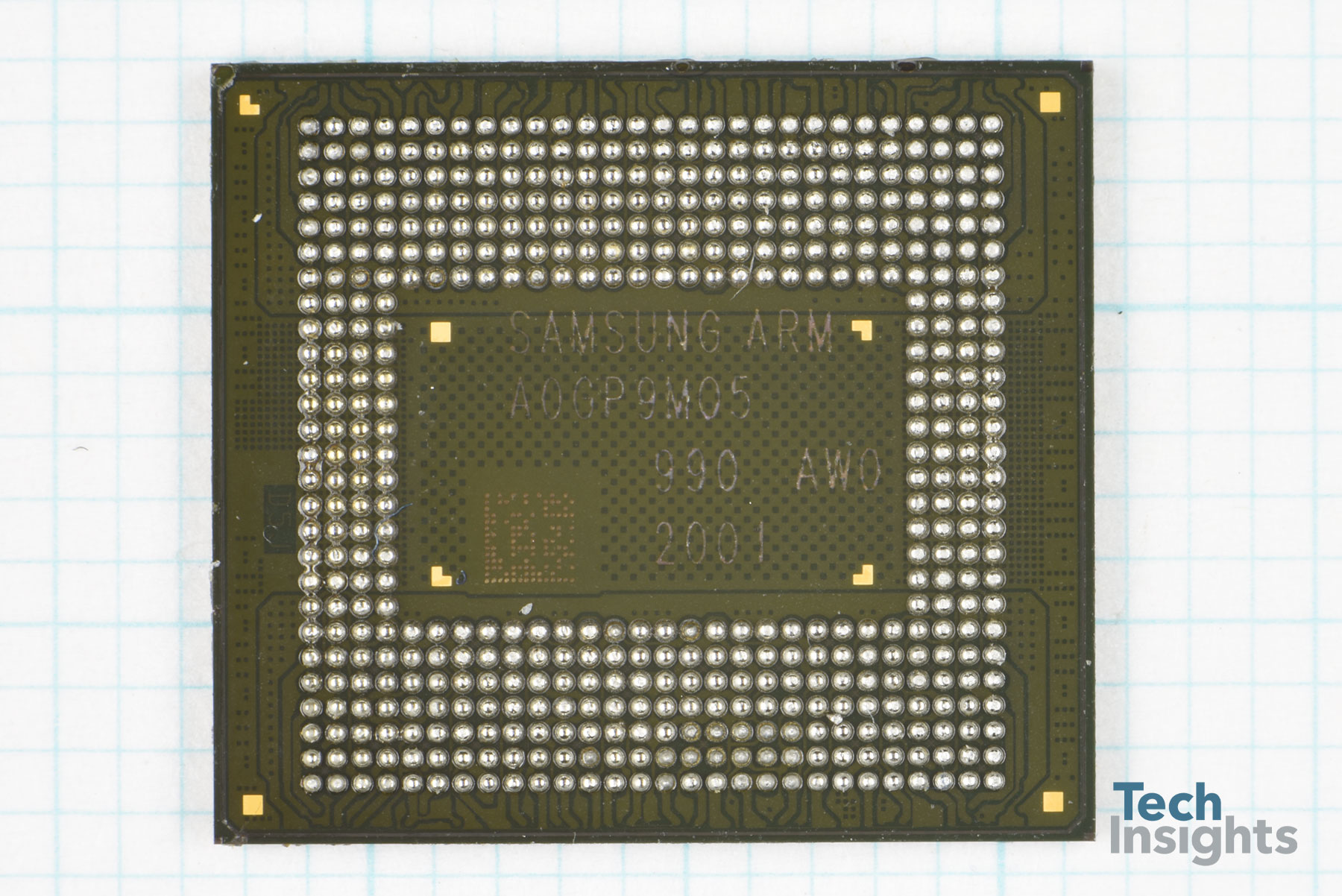
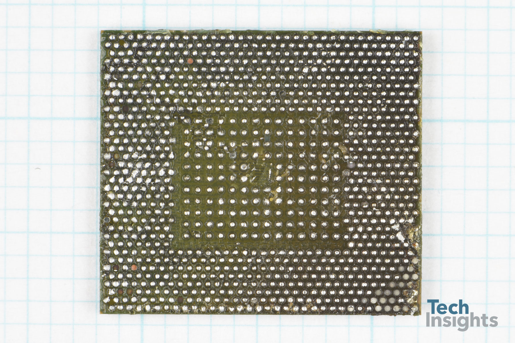
The Exynos 990 Application Processor is fabbed in Samsung 7nm LPP EUV; it is the third Samsung 7LPP EUV fabbed part we have seen, after the Samsung Exynos 9825 and Qualcomm Snapdragon 765G SoCs. TechInsights will examine the Exynos 990 Samsung 7LPP EUV process.
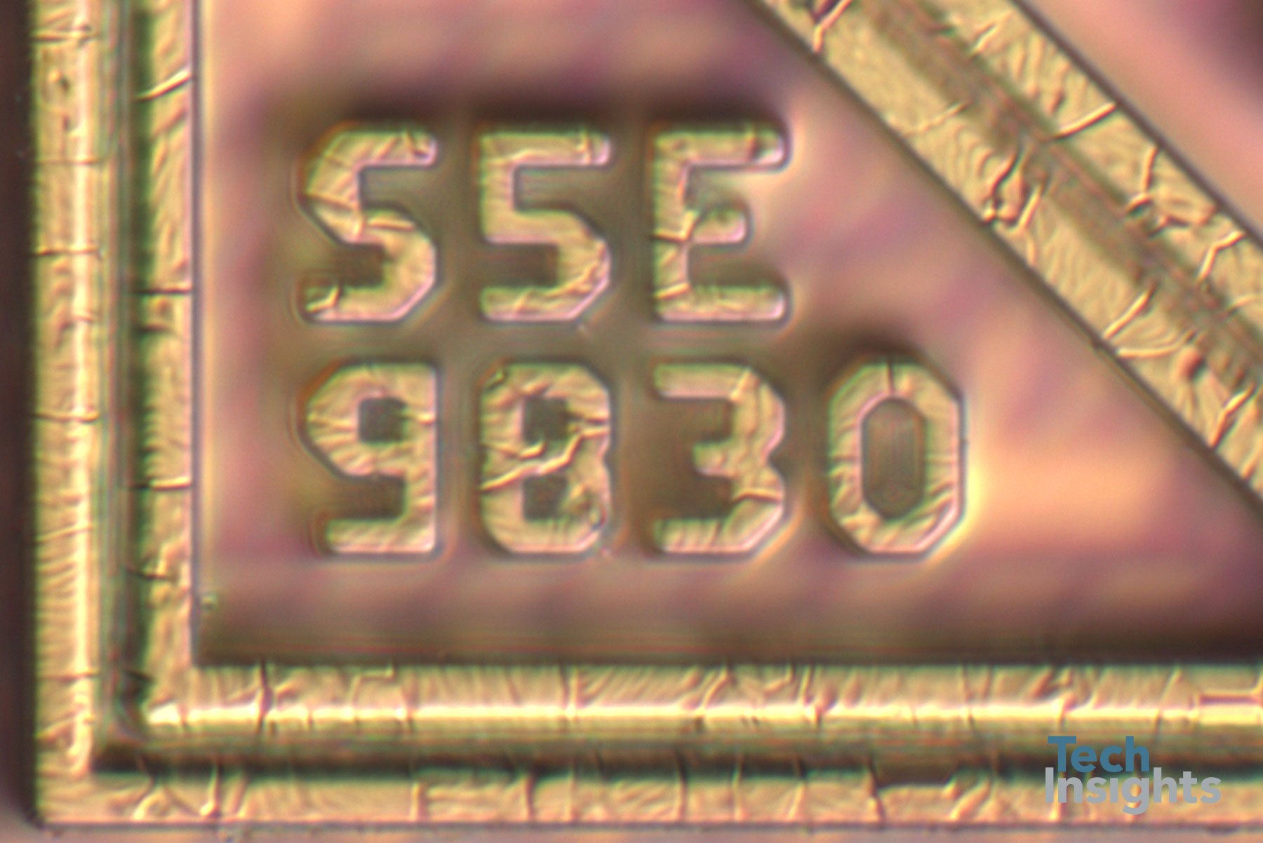
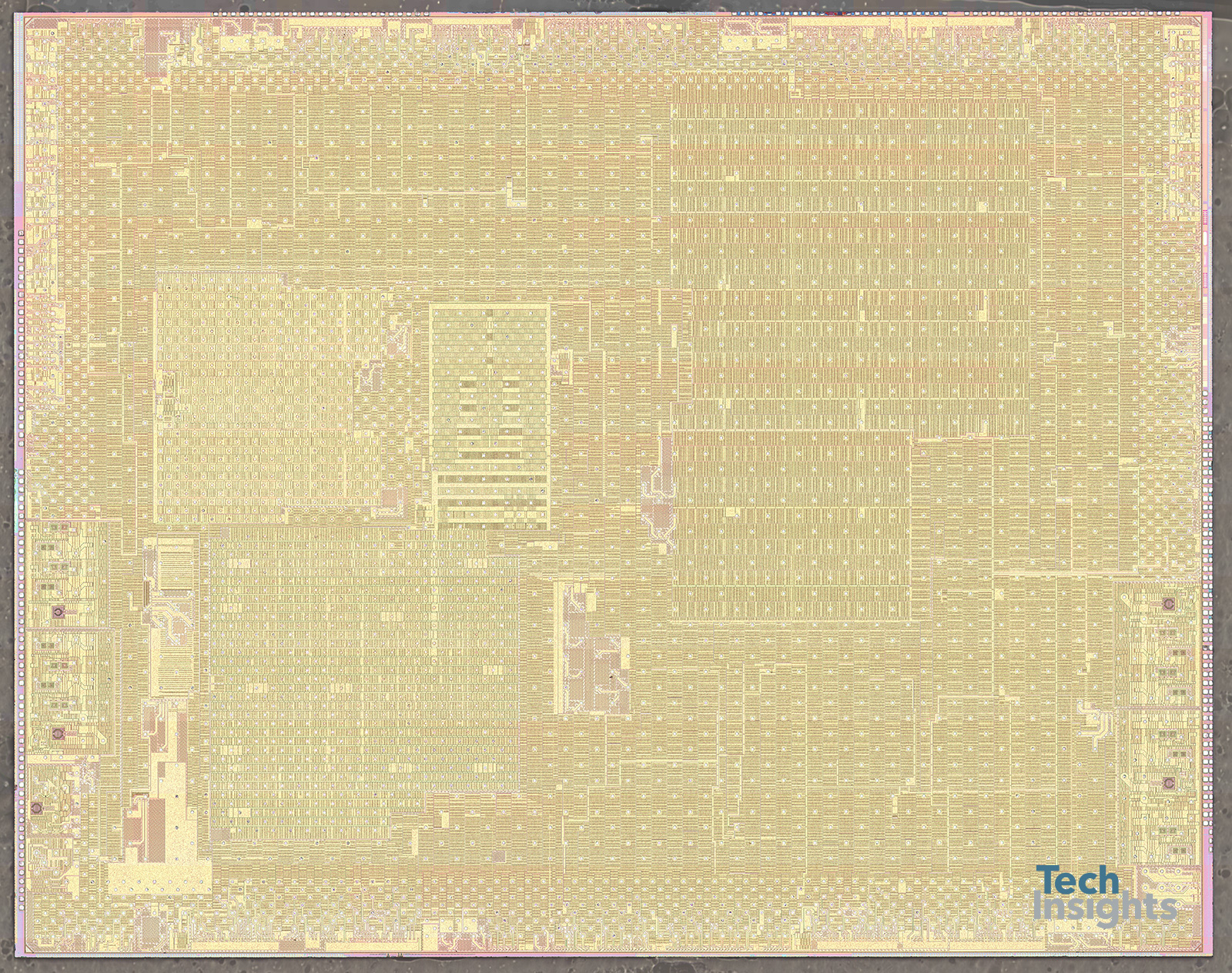
The Samsung Exynos 990 Application Processor die S5E9830 has a die size (seal) of 10.74 mm x 8.55 mm = 91.83 mm2. Since it is a pure Application Processor without modem, its die size cannot be directly compared to their previous Exynos 9825 or Exynos 980, which are 4G SoC and 5G SoC respectively.
Analysis Continues
We will be working on Samsung Galaxy S20 Ultra 5G for some time.
There is a lot of new silicon included in this flagship series phone; we will be analyzing different parts of this phone under several of our subscriptions, including Memory, Logic, Mobile RF, Power Semiconductor, and IoT SoC.
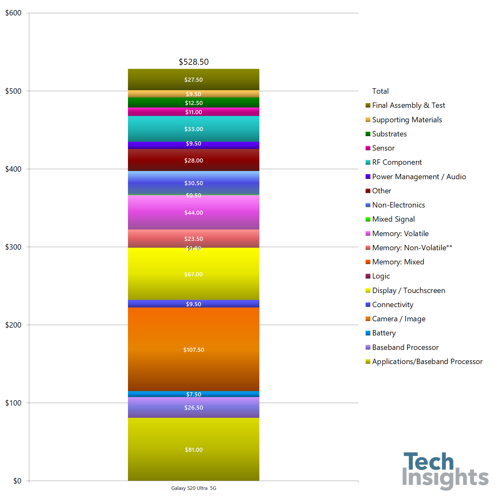
In the near future, we will be adding more of our findings to this blog. Plans include further discussion of design wins, publishing die photos, and providing high level costing for the components found in the phone.


