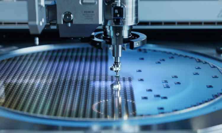
- Selected teardown photographs, package photographs, package X-rays, die markings, and die photographs
- Scanning electron microscopy (SEM) cross-sectional micrographs of the general structure of the die dielectric materials, major features, and transistors
- Measurements of vertical and horizontal dimensions of major microstructural features
- Plan-view optical micrograph of the die delayered to the polysilicon layer
- Identification of major functional blocks on a polysilicon die photograph
- Table of functional block sizes and percentage die utilization
- High-resolution image signal processor (ISP) polysilicon die photographs delivered in CircuitVision
- Cost of tested die, based on the cost analysis of the observed process
The image set for a standard project is derived from decapsulation of two samples, followed by SEM analysis of a cross section of the ISP die and optical layout analysis of the ISP die delayered to the gate level.


