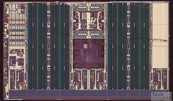
This report contains the following detailed information:
- Selected teardown photographs, package photographs, package X-rays, die markings, and die photographs
- SEM cross-sectional micrographs of the general structure of the die dielectric materials, major features, and transistors
- SEM plan-view micrographs at active, word line (WL), and bit line (BL) levels from a beveled sample
- Measurements of vertical and horizontal dimensions of major microstructural features
- Plan-view optical micrograph of the die delayered to the polysilicon layer
- Identification of major functional blocks on a polysilicon die photograph
- Table of functional block sizes and percentage die utilization
- High-resolution top metal and diffusion level die photographs delivered in the CircuitVision software
The authoritative information platform to the semiconductor industry.
Discover why TechInsights stands as the semiconductor industry's most trusted source for actionable, in-depth intelligence.
1891 Robertson Rd #500, Nepean, ON K2H 5B7
Copyright © 2024 TechInsights Inc. All rights reserved.


