Posted: October 30, 2018
Contributing Author: Sinjin Dixon-Warren, PhD
MicroVision, based in Redmond WA, now in partnership with STMicroelectronics, has been a technology leader in the small form factor laser beam scanning (LBS) projector market. Recently, TechInsights analysed samples of two consumer projects based on the MicroVision-STMicroelectronics LBS projector technology, which is marketed under the PicoP® scanning technology brand. Here, we will summarize some of the results of our reverse engineering of this ingenious technology.
The PicoP technology is presently found in the MP-CL1A mobile projector from Sony and in the VOGA V projector phablet from China-based Ragentek. TechInsights found the MP-CL1A to contain a 5-laser MicroVision module, while the VOGA V contains a 3-laser module. Both projectors used the same STMicroelectronics-fabricated magnetically-actuated scanning silicon mirror die. This article focuses on the Sony device.
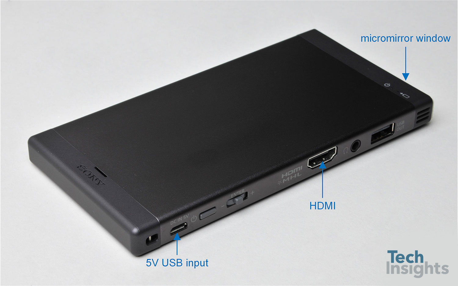
Figure 1: Sony MP-CL1A Projector – Tilt View

Figure 2: Sony MP-CL1A Projector – Front View
The MP-CL1A is compact, with dimensions 77 mm x 15o mm x 14 mm thick is shown in Figure 1. It is powered using a 5 V USB cable and has a standard HDMI input and a USB output. The front face of the projector, shown in Figure 2, features a window through which the scanning micromirror can easily be seen with the naked eye.
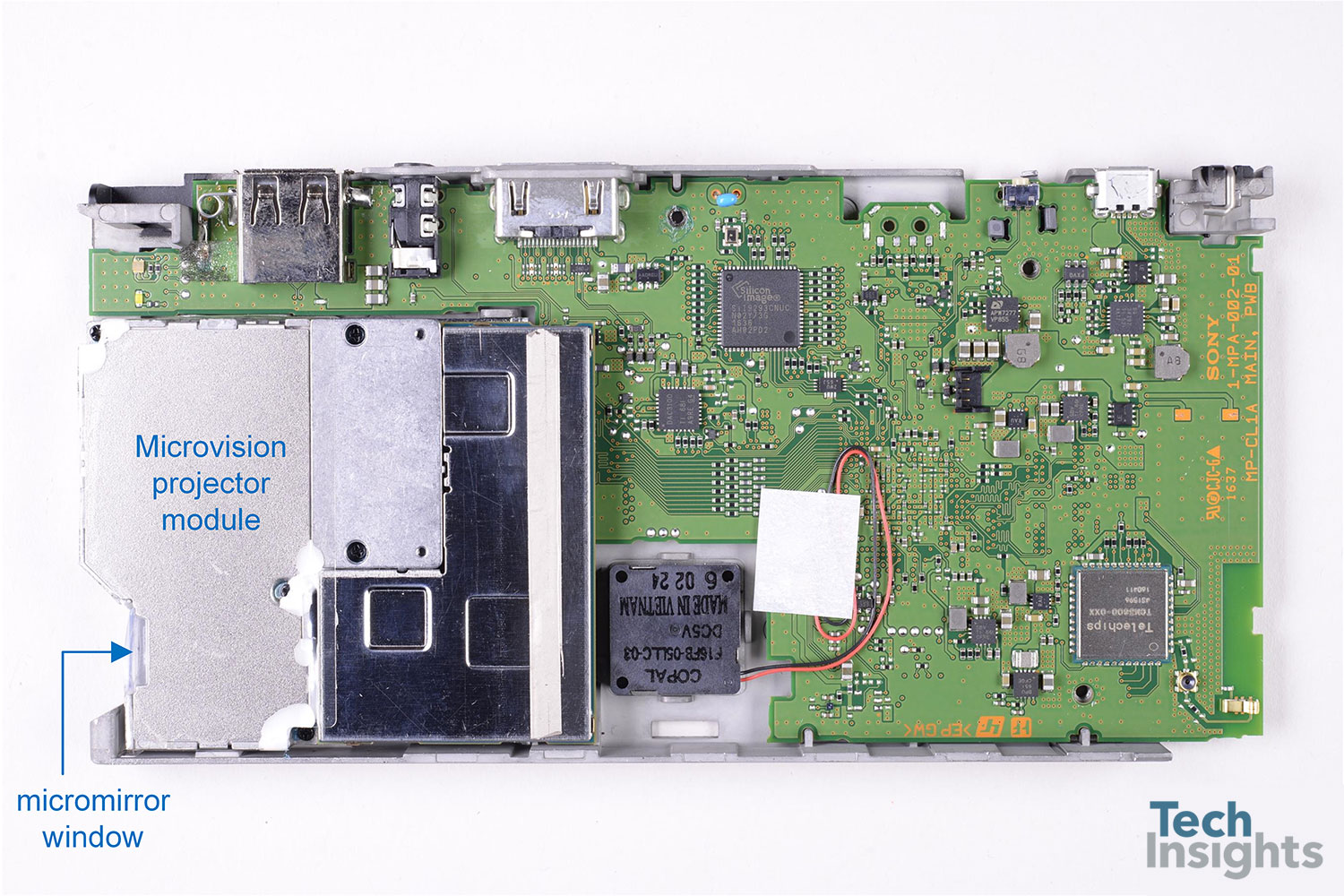
Figure 3: Sony MP-CL1A Projector Main PCB
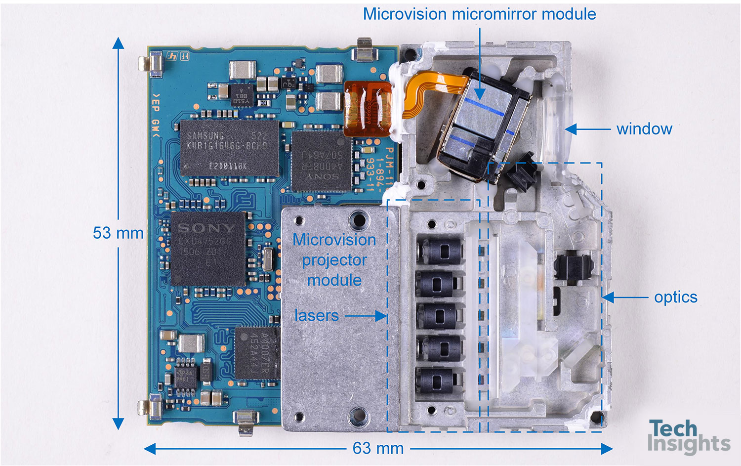
Figure 4: Sony MP-CL1A Projector Module
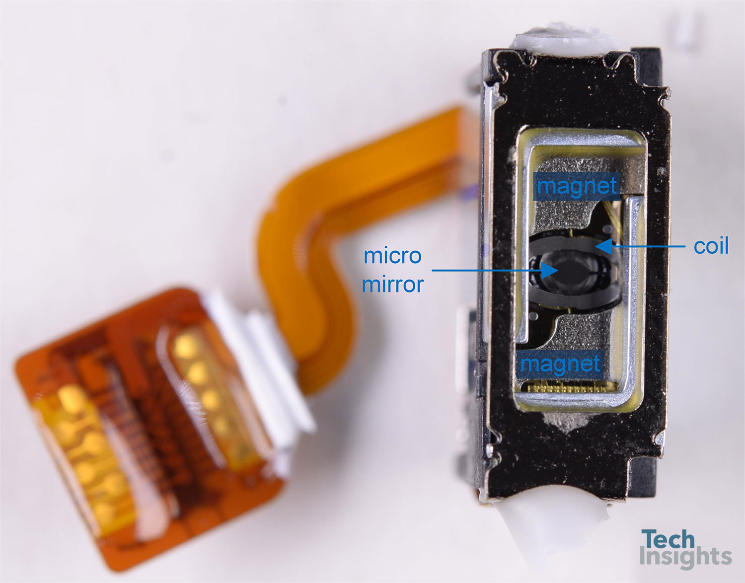
Figure 5: MicroVision Micromirror Module – Front View
Teardown of the device revealed a main PCB manufactured by Sony and the MicroVision projector module, which is mounted on the left end of the PCB, as shown in Figure 3. The micromirror window is located at the bottom left corner of the image.
The internal workings of the 53 mm x 63 mm projector module were revealed by removal of the metal shield. The module, shown in Figure 4, features five lasers, likely two red, two green and one blue, an optical combiner and various other lenses that col-sm-12 col-lglimate the light. The combined laser beam is then reflected off the micromirror and out through the window. The operation of the projector depends on synchronous modulation of the five lasers and scanning of the mirror in a raster pattern. The pairs of red and green lasers are used to reduce the effects speckle in the projected image.
Removal of the MicroVision micromirror module allowed us to take a closer look at the silicon micromirror. The micromirror is suspended on torsion springs from a frame with a Lorentz coil, as can be seen in Figure 5. The silicon die is surrounded by permanent magnets. As is discussed in more detail below, the micromirror is actuated into a raster motion by passing an AC current through the Lorentz coil.
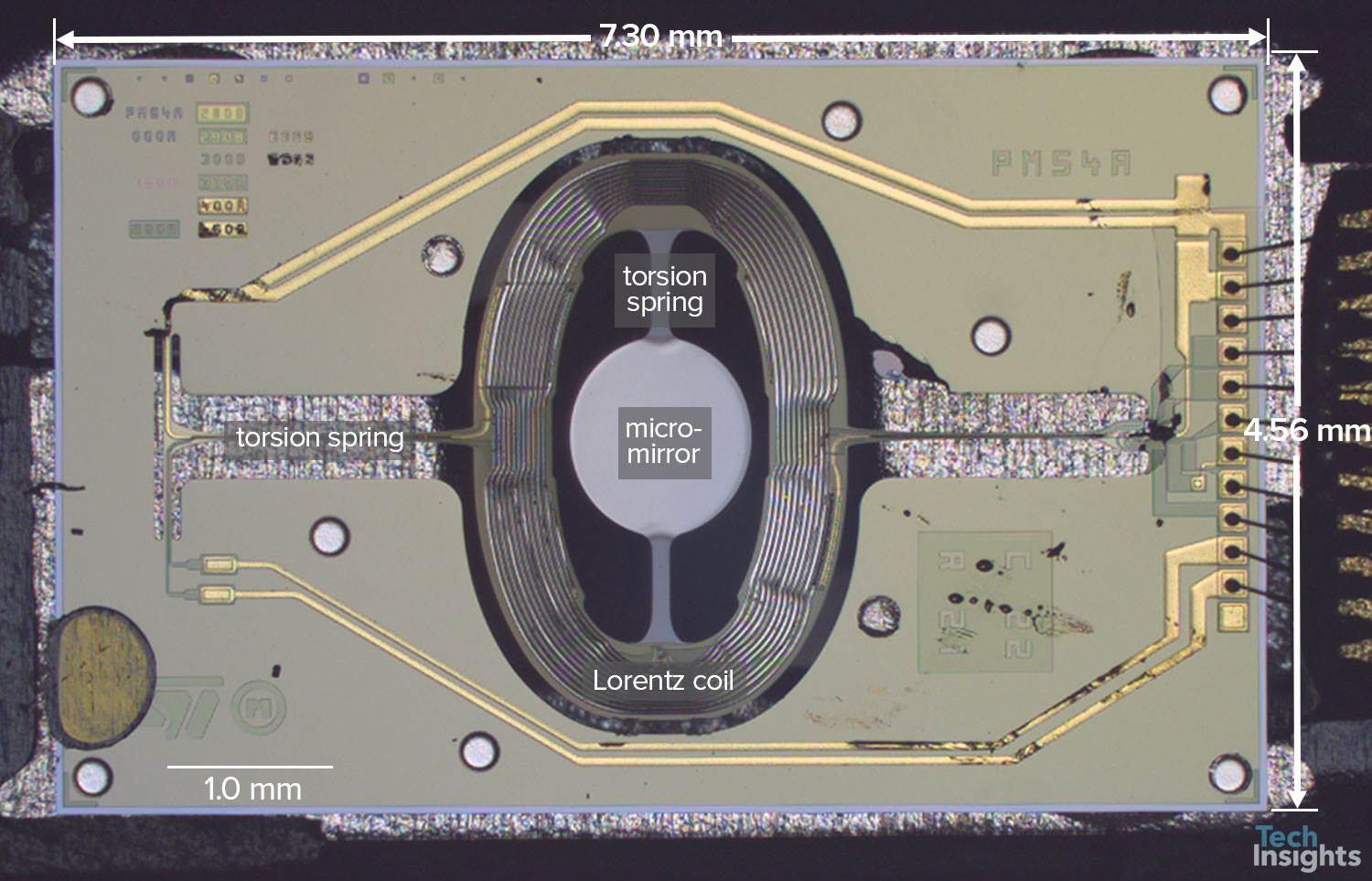
Figure 6: MicroVision/STMicroelectronics PM54A Micromirror Die
Techinsights was able to remove an intact PM54A die from one of the projector modules, as shown in Figure 6. The die is 7.30 mm x 4.56 mm, and is quite clearly fabricated by STMicroelectronics based on MicroVision’s technology. It features a central micromirror mounted by vertically-oriented torsion spring to an outer frame. The outer frame features a Lorentz coil and is mounted by horizontally-oriented torsion springs to the die substrate. Simple inspection demonstrates that the two sets of torsion springs will allow the mirror to tilt in two orthogonal directions, thus allowing for the required raster motion of the reflected laser beam.
Two other features of note are Wheatstone Bridge strain sensor structures located at the bottom end of the inner torsion springs and the right end of the right-hand outer torsion spring, as shown in Figure 7 and Figure 8. These two sensors provide feedback to the controller that drives current through the Lorentz coil.
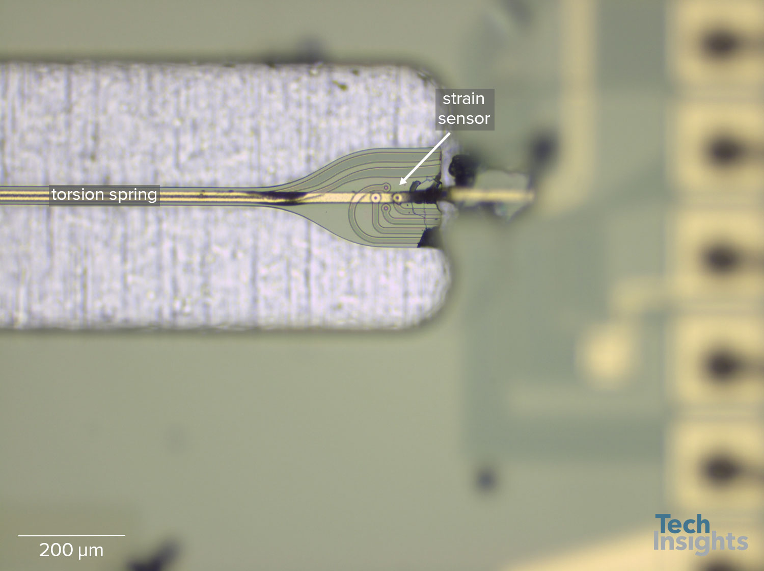
Figure 7: STMicroelectronics/MicroVision PM54A Outer Torsion Spring and Strain Sensor Detail
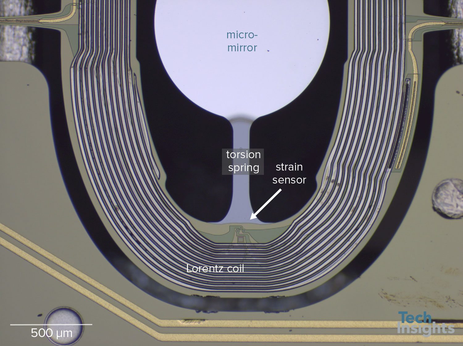
Figure 8: STMicroelectronics/MicroVision PM54A Inner Torsion Spring and Strain Sensor Detail
The mode of operation of the magnetically actuated MicroVision micromirror devices is described in US Patent US20100079836A1. Figure 9 shows Fig. 3 from the patent. The following text describes how the application of an AC drive current can induce motion of the micromirror along the two orthogonal axes of rotation for the micromirror:
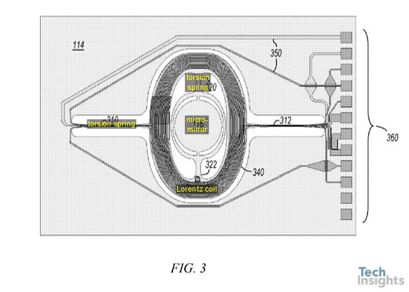
Figure 9: US Patent 20100079836 A1 (Fig. 3)
FIG. 3 shows a plan view of a scanning platform with a microelectromechanical system (MEMS) scanning mirror. Scanning platform 114 includes gimbal 340 and scanning mirror 116. Gimbal 340 is coupled to scanning platform 114 by flexures 310 and 312, and scanning mirror 116 is coupled to gimbal 340 by flexures 320 and 322. Gimbal 340 has a drive coil connected to drive lines 350. Current driven into drive lines 350 produces a current in the drive coil. Scanning platform 114 also incorporates one or more integrated piezoresistive position sensors. In some embodiments, scanning platform 114 includes one position sensor for each axis. Two of the interconnects 360 are coupled to drive lines 350. The remaining interconnects provide for the integrated position sensors for each axis.
In operation, an external magnetic field source (not shown) imposes a magnetic field on the drive coil. The magnetic field imposed on the drive coil by the external magnetic field source has a component in the plane of the coil, and is oriented at roughly 45° with respect to the two drive axes. The in-plane current in the coil windings interacts with the in-plane magnetic field to produce out-of-plane Lorentz forces on the conductors. Since the drive current forms a loop on gimbal 340, the current reverses sign across the scan axes. This means the Lorentz forces also reverse sign across the scan axes, resulting in a torque in the plane of and normal to the magnetic field. This combined torque produces responses in the two scan directions depending on the frequency content of the torque.
The MicroVision micromirror MEMS technology is an exquisite example of MEMS engineering and design. TechInsights has additional analysis available on this technology, including cross-sectional analysis of the MEMS die, which is summarized in our recent report here.


