Posted: November 15, 2013
Sony PlayStation 4
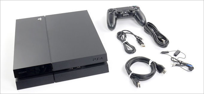
Sony’s PlayStation 4 makes its debut today and TechInsights’ Teardown team has hands on analysis of the components that promise to set a new benchmark in the gaming industry. While we’ll be tearing down the Microsoft’s XBOX ONE next Friday, today we take and in-depth look at the chips and components in the PS4.
You’d think that in seven years, Sony would incorporate a fair bit of design innovation and that is in fact what we have here. In that time span, the market has evolved from gaming consoles to full fledged living room hubs that incorporate games, movies, music, social and much more. Despite the home media revolution, Sony’s marketing messaging has made it very clear that the PS4 is first and foremost a gaming console.
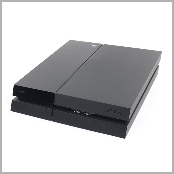
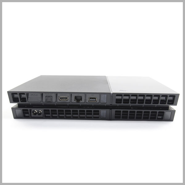
The new PS4’s design blends Sony’s traditional jet black color with a slim and lustrous look. It’s very similar in size to Sony’s second generation PS3 and slightly more compact than its rival Xbox One. One of the first things we noticed was that Sony’s engineers managed to find a way to fold the power supply inside the box, leaving clumsy gamers with no peripheral power brick to trip over.
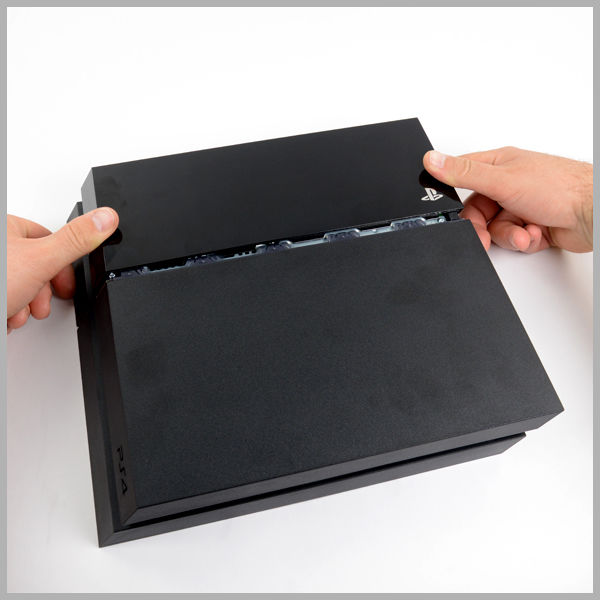
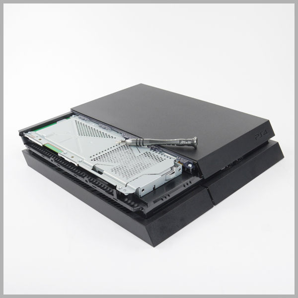
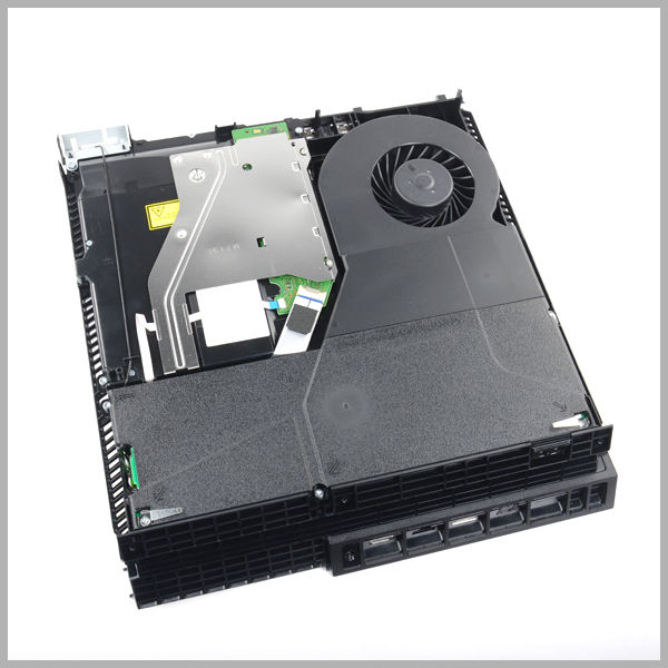
Inside the Sony PlayStation 4
What's Inside?
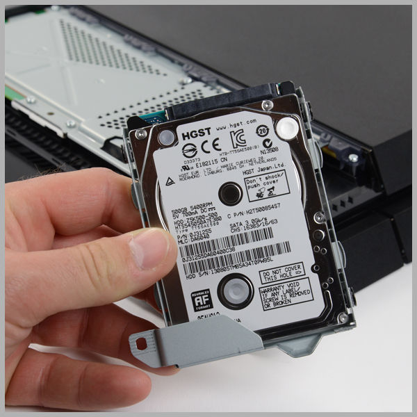
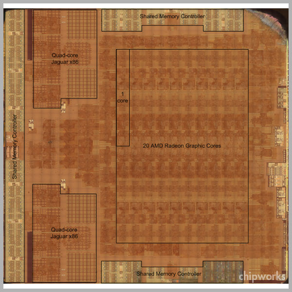
We know for sure that the PS4 is powered by a single chip custom CPU/GPU processor including a low power x86-64 AMD 8 core CPU block and a 1.84 TFLOPS AMD Radeon GPU block packaged in this single SoC. We also expected to find 8 GB GDDR5 RAM, 500 GB removable and upgradable hard drive storage, 802.11 b/g/n Wireless and Bluetooth 2.1 and USB 3.0 + Ethernet 10/100/1000.
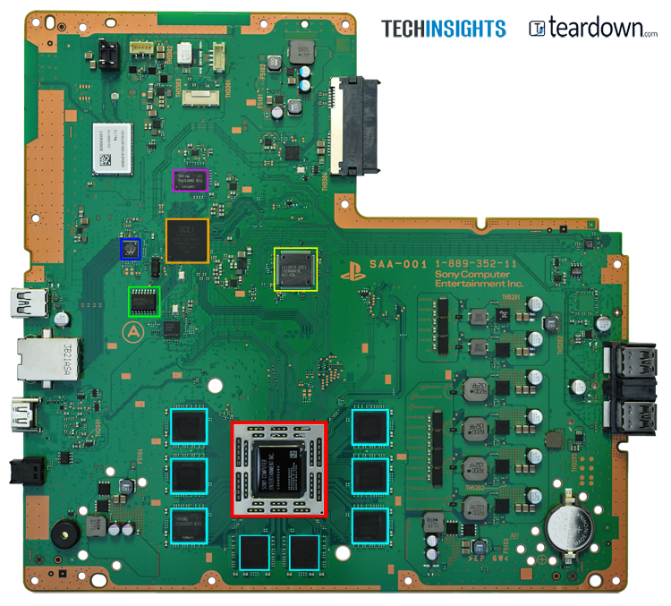
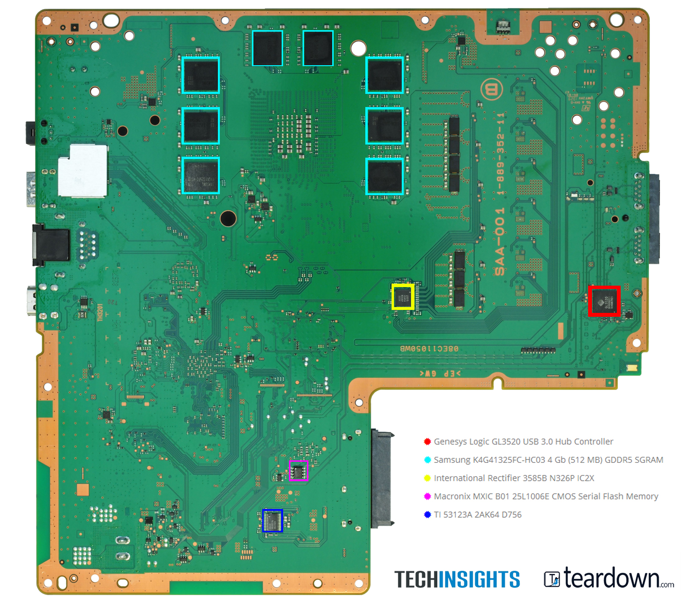
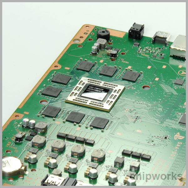
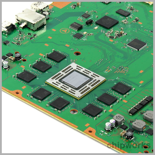
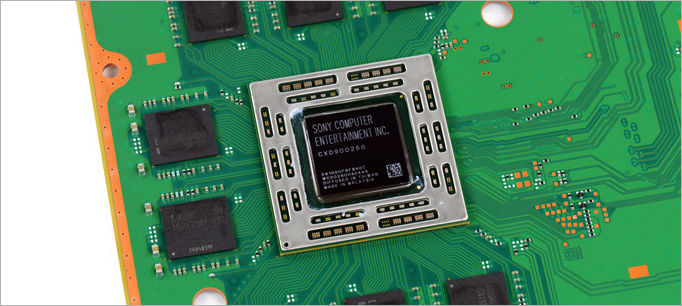
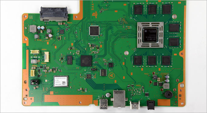
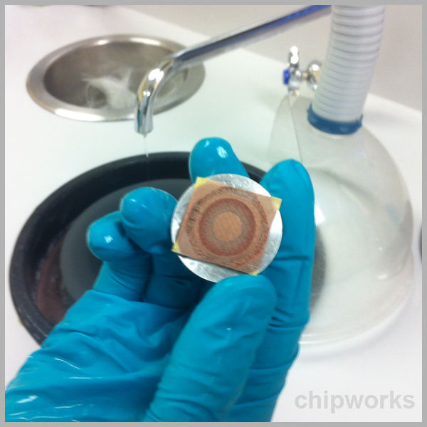
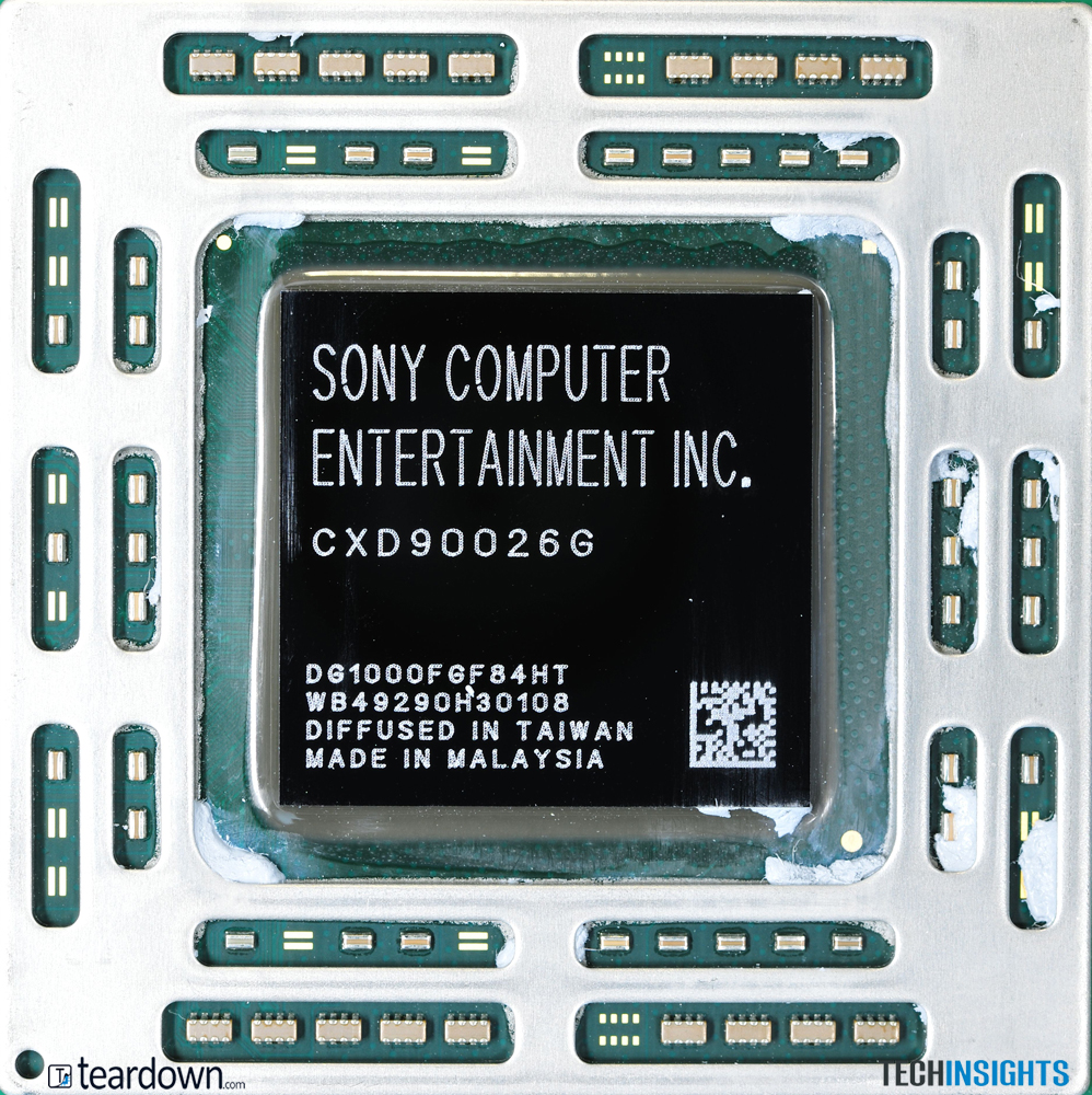
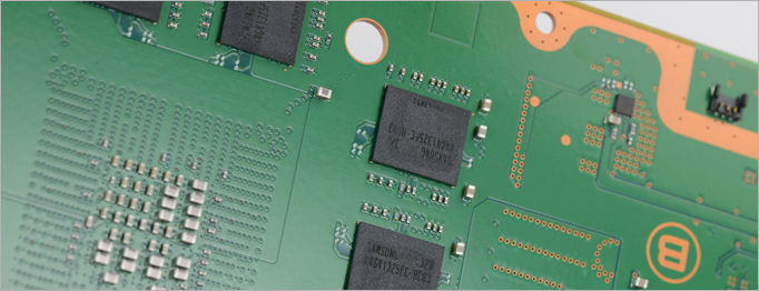
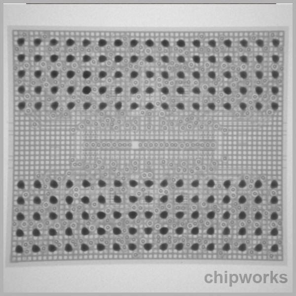
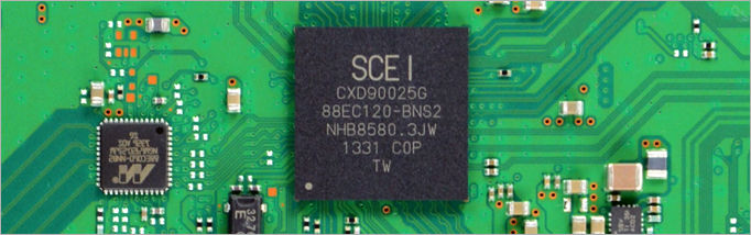
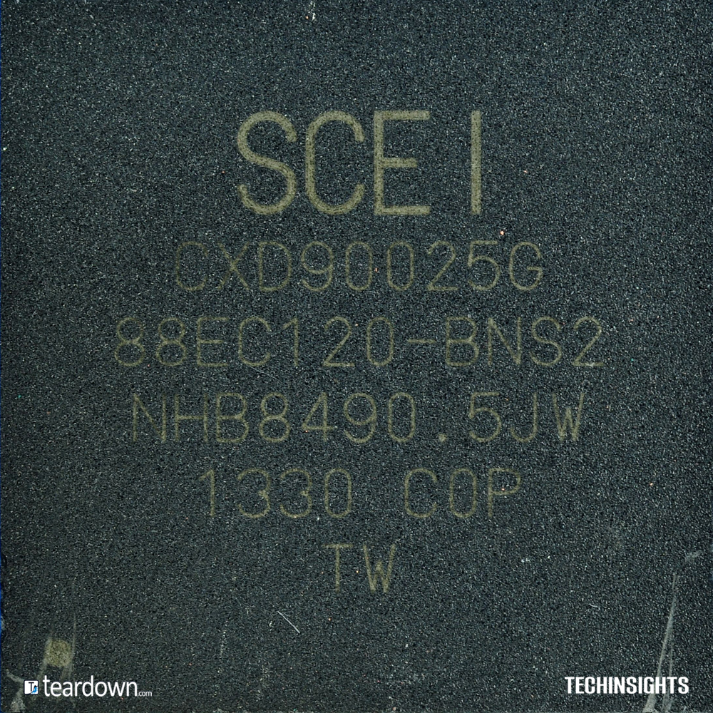
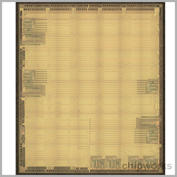
The Main Processor
The Main Processor
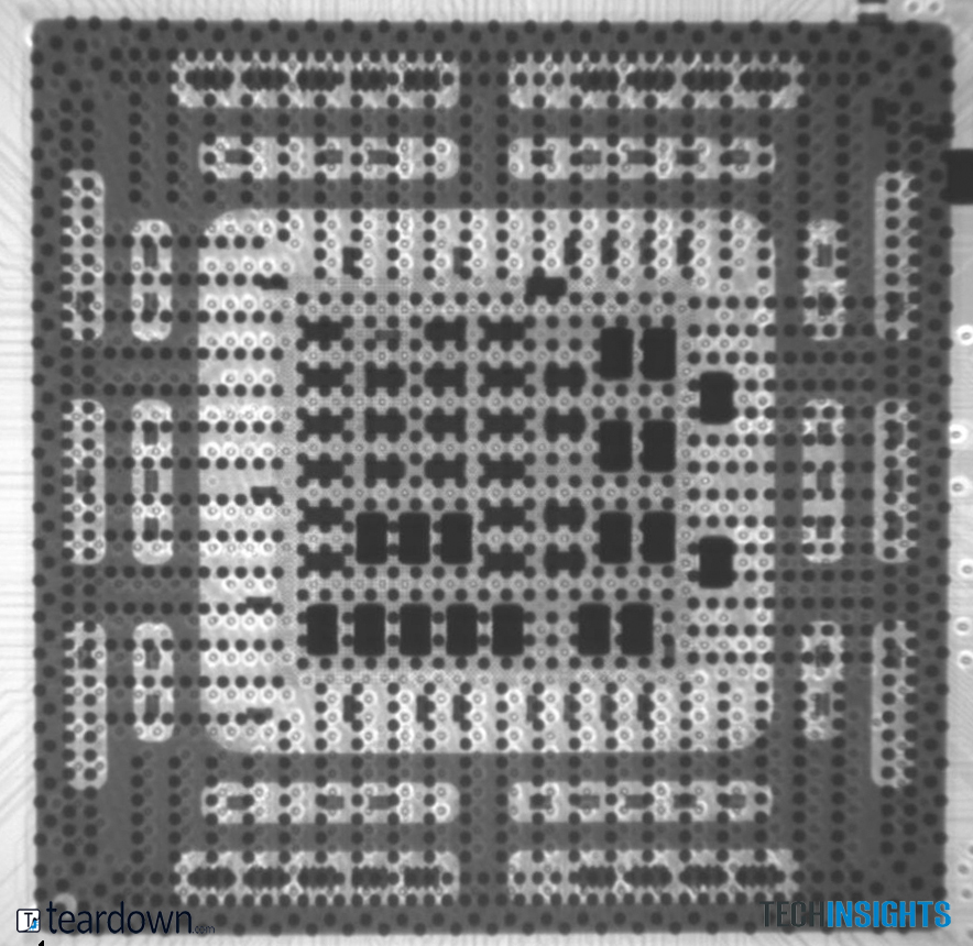
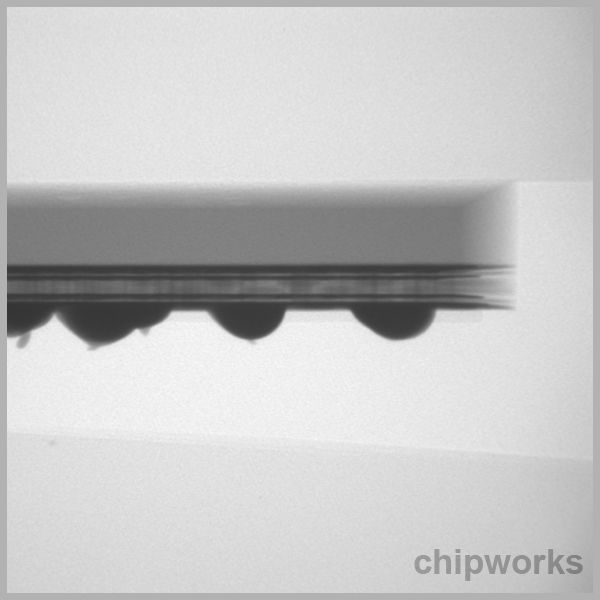
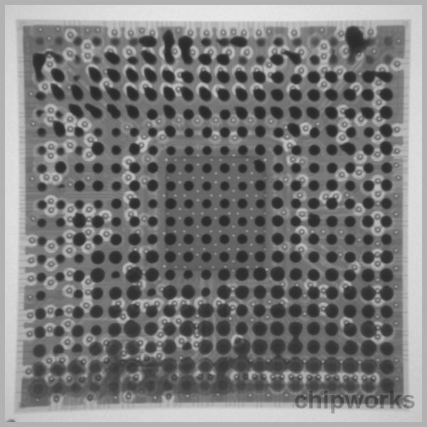
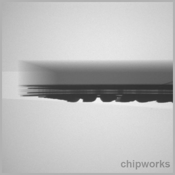
Based on widely circulated information, the PS4 uses a single die CPU/GPU and one main shared 8GB memory array. We therefore expected to see a single die under the main processor package, with no separate DRAM die in package, and no embedded DRAM on the main die. This is indeed what we have found. A huge monolithic die of 19 x 18.3 mm.
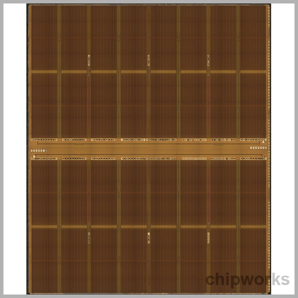
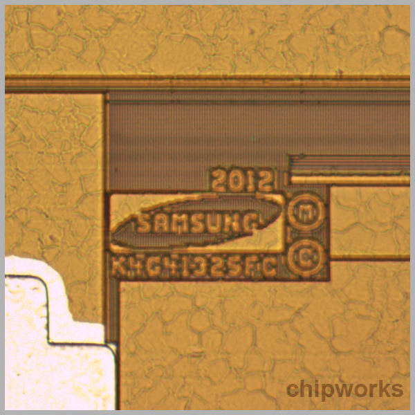
DRAM
The DRAM
Many readers will have seen Sony’s own teardown video of the PS4. From the view of the mainboard seen in this video, one might have expected the eight DRAM die visible on the top of the board to be eight 1GB DRAM ICs. In fact there are eight DRAM ICs on the top of the board and eight on the bottom of the board. Given Sony’s published specs giving the amount of main memory at 8GB, we can conclude that each of the 16 DRAM die are 512MB.
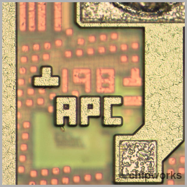
Network Co-Processor
The Network Co-Processor
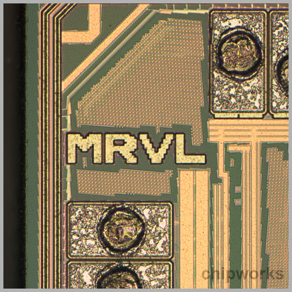
One of the convenient new features of this generation of console is the capability they have to download content while in standby mode. This is enabled by dedicating silicon to that specific task, such that the majority of sub-systems can be turned off while keeping that functionality alive. The PS4’s dedicated network processor appears to be a custom ASIC by Marvell, judging from the package markings.
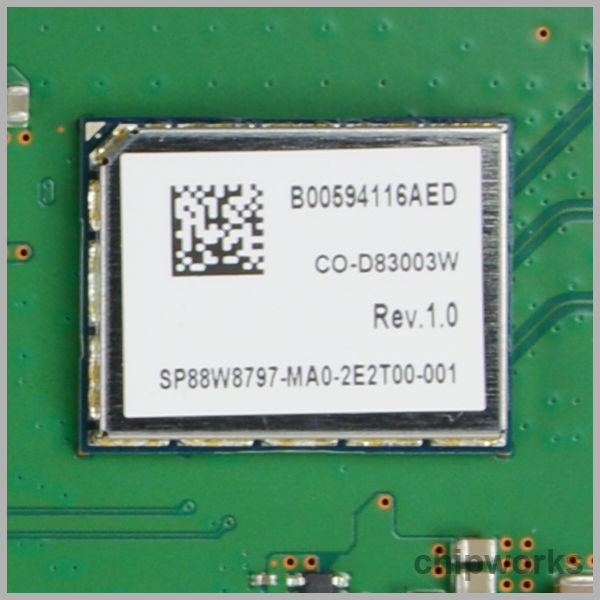
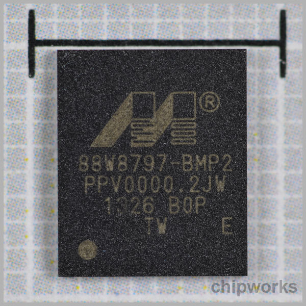
WiFi Module
The WiFi Module
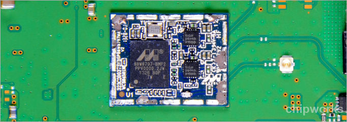
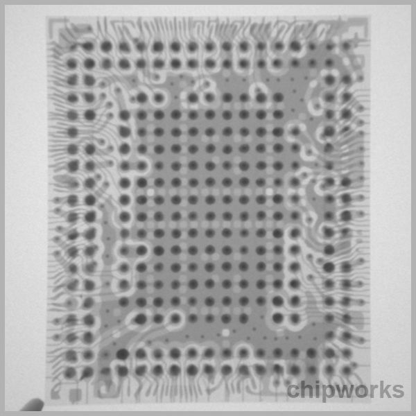
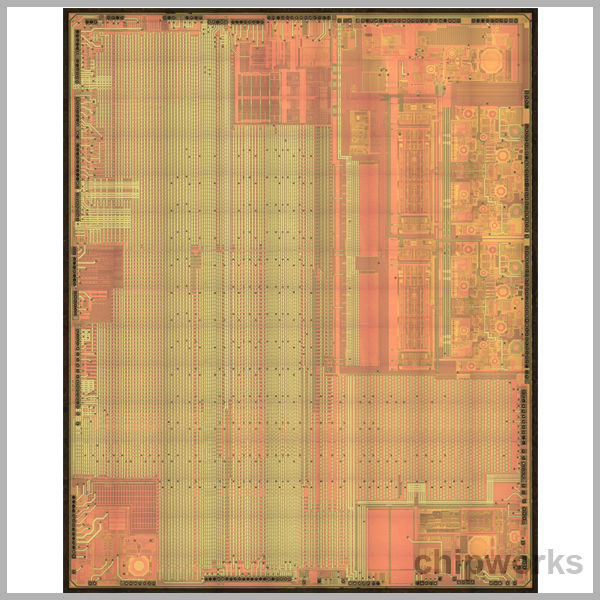
The WiFi Module featuring a metal lid and Marvell package markings contains an interesting component. The WiFi engine behind the PS4 is a Marvell Avastar 88W8797. The Avastar features multiple-input multiple-output (MIMO) Wi-Fi 802.11 a/b/gn/ + Bluetooth 4.0 with Low Energy Support (BLE) plus FM radio and an embedded PMIC block. Interestingly, this Avatar was designed for mobile applications like smart phones and tablets, but to date Chipworks has only ever observed this Marvell device inside one other product, The Microsoft Surface Tablet back in October of 2012. Do you think Sony got a deal on this? The WiFi module also contains two Skyworks/SiGe WiFi front end modules. The Avastar die measures 5.6 x 6.9 mm and was fabricated at TSMC and appears to be fabricated on a 65 nm mixed signal process technology.
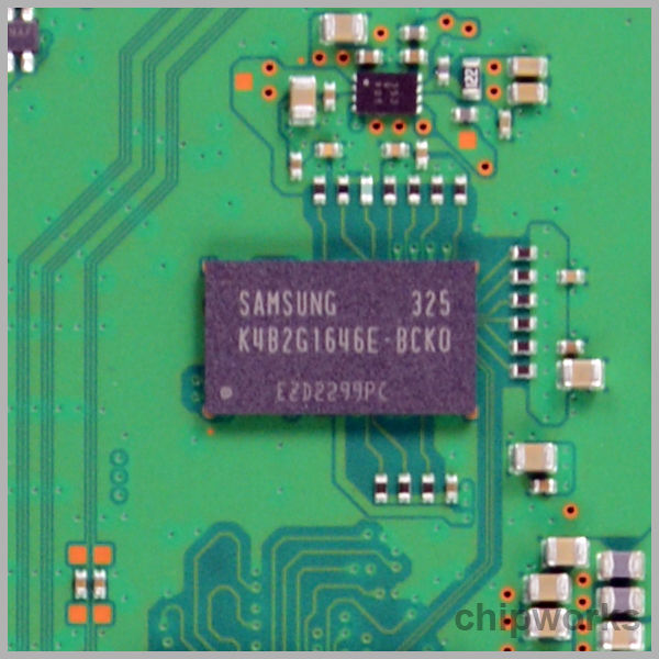
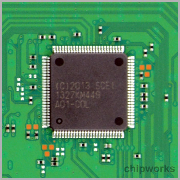
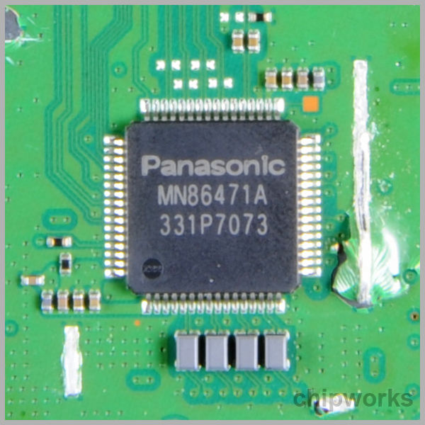
Other Devices of Interest
The remaining major components found tonight include Samsung 2G DDR 3 SDRAM used by the network co-processor, Sony Computer Entertainment Inc. (SCEI) device marked only as “1327KM449” and Panasonic's MN86471A HDMI Communication LSI.
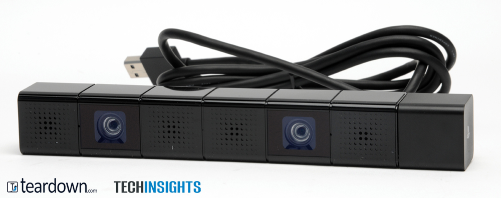
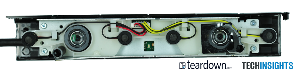
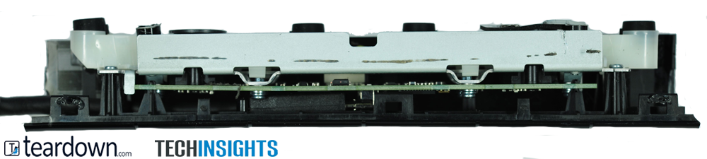
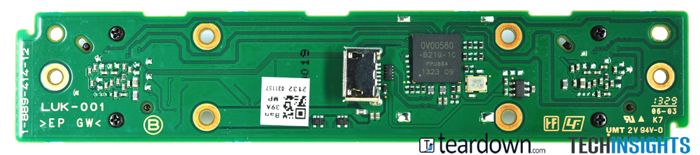
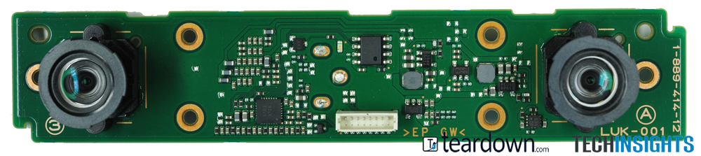
PlayStation Camera
PlayStation Camera
The PlayStation 4 Camera, initially named PlayStation 4 Eye, is a motion sensing input device. It includes two 1280×800px cameras. The lenses will operate with an aperture of f/2.0, with 30 cm focusing distance, and an 85° field of view.
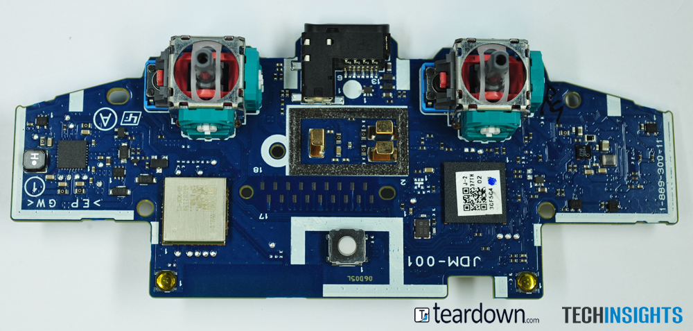
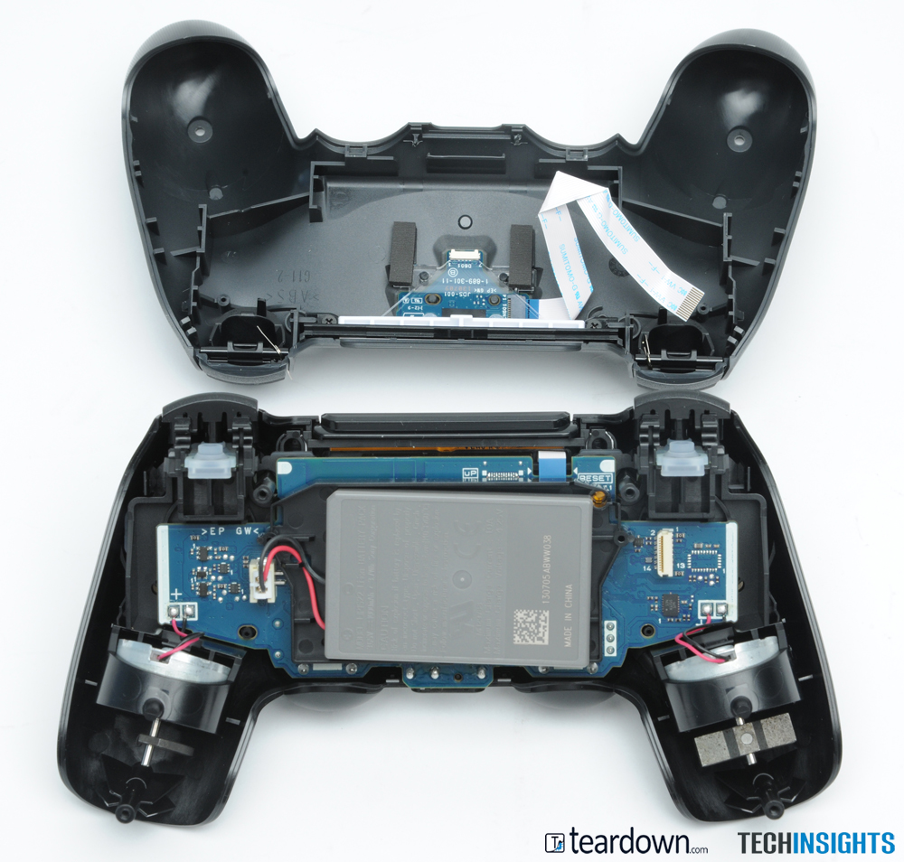
DualShock 4 Controllers
DualShock 4 Controllers
Our teardown also includes teardown of the new DualShock 4. The DualShock 4 is the PlayStation 4's primary controller and while to the DualShock 3 it connects to the console via Bluetooth 2.1+EDR.
These IC support the PS4’s new features, including a built-in two-point capacitative touch pad on the front of the controller and support motion detection via a three-axis gyroscope and three-axis accelerometer and improved vibration.