Posted: June 13, 2017
Contributing Authors: Ray Fontaine
This year’s IISW marked the 10th anniversary of this biennial conference and corresponded to the 10th anniversary of TechInsights’ presence at the workshop. Don Scansen attended in 2007, under the Semiconductor Insights banner, and gave a poster presentation on image sensor trends. Chipworks attended and gave oral presentations in 2009, 2011, 2013, 2015, and now that the TechInsights/Chipworks merger is complete, again in 2017 as TechInsights.
The workshop itself is an extension of the IEEE-sponsored Workshop on CCDs and Advanced Image Sensors going back to 1986. It’s a gathering of the technologists in the imaging community where substantial time is given for Q/A sessions after the oral presentations, fostering a true workshop atmosphere. It’s no small feat to organize the workshop, attended by ~180, and a great credit to the board of directors, technical program chair/committee, and sponsors, all of whom run the workshop in their spare time.
The 2017 papers have a planned release to the imagesensors.org website sometime in August 2017. Until then, we thought it would be worthwhile to share portions of the TechInsights paper and selected presentation material in a series of blog postings. The first contribution will focus on phase detection autofocus (PDAF) systems and will be followed by chip stacking and pixel isolation structures over the coming weeks. So, without further ado, part 1:
A Survey of Enabling Technologies in Successful Consumer Digital Imaging Products (Part 1: PDAF)
Abstract—The image quality and customized functionality of small-pixel mobile camera systems continues to bring true product differentiation to smartphones. Recently, phase detection autofocus (PDAF) pixels, pixel isolation structures, chip stacking and other technology elements have contributed to a remarkable increase in mobile camera performance. Other imaging applications continue to benefit from small-pixel development efforts as foundries and IDMs transfer leading edge technology to active pixel arrays for emerging imaging and sensing applications.
Index Terms—CMOS image sensor, through silicon via, Cu-Cu hybrid bonding, direct bonding interconnect, homogeneous wafer-to-wafer bonding (oxide bonding), stacked chip, phase detection autofocus, image signal processor
I. Introduction
CMOS image sensor (CIS) pixel scaling has nearly ended, and indeed some smartphone camera development teams have reversed the pixel scaling race in favor of larger pixels with increased full well capacity. Nevertheless, the pace of image sensor technology development seems to be increasing. The era of chip stacking is well underway and offers increased flexibility in terms of manufacturing and systems partitioning. The state-of-the-art smartphone camera chips feature a pixel pitch down to 1.0 µm and up to 23 MP resolution. Dual cameras are becoming popular, including the availability of products featuring dual front- and rear-facing cameras. PDAF systems now employ three distinct and complementary techniques: contrast, phase, and laser-assisted ranging. At the chip level, evolutions in direct bond interconnect (DBI) and deep trench isolation (DTI) are facilitating the performance gains realized by recent stacked imaging chips.
II. PDAF
Conventional, passive AF systems relied on contrast-only techniques until locally masked PDAF pixel apertures were added to active pixel arrays to facilitate hybrid (contrast and phase) AF systems. It is a fortunate circumstance that nearly all observed masked PDAF pixels to date require little additional processing during chip fabrication, only the repurposing of existing structures to serve as PDAF pixel aperture masks.
Examples of both half-masking, in which neighboring PDAF pixel pairs are simply 50% masked, and variable pixel aperture window sizes have been found in use. The early trend for both types of masked PDAF pixels was to deploy them within a relatively small central region of the active pixel array, or as linear arrays (periodic rows of PDAF pixel pairs). Today, masked pixel PDAF arrays in marquee products occupy more than 90% of the host active pixel arrays and display a trend of increasing density generation-over-generation.
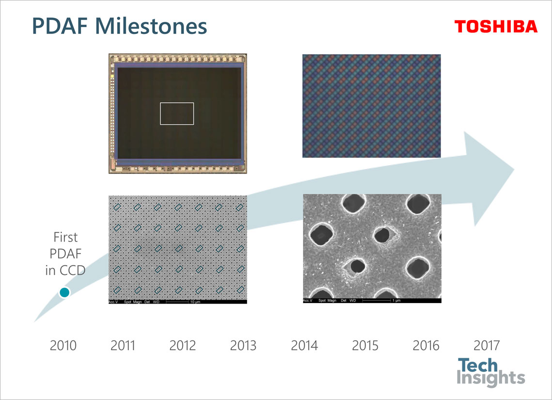
PDAF Milestones
A. Masked PDAF in Front-Illuminated CCDs
Hybrid PDAF systems were introduced to the camera market by a FujiFilm press release in July 2010. The FinePix Z800EXR featured a hybrid AF system with a stated AF performance of 0.158 s [1]. This front-illuminated charge-coupled device (CCD) imager, fabricated by Toshiba, employed metal half-masks in two of 32 pixels within a rectangular PDAF subarray occupying the central ~7% of the active pixel array [2]. In the case of the CCD structure, the W-based shielding metal, already in use in conventional CCDs, was patterned to form PDAF half-masks just above the photodiode (PD) region.
B. Masked PDAF in Front-Illuminated CMOS
Half-masked front-illuminated CMOS PDAF pixels were first noted in the Nikon V1, announced in September 2011 [3]. The Aptina-sourced chip featured PDAF pixels implemented as nine linear arrays configured as evenly spaced rows across the active pixel array [4]. The PDAF pixel row segments were all green channel pixels and the aperture mask was implemented in metal 1 (Cu). Alternating pixels within the row segment featured right/left masks.
Variable aperture masks emerged in 2012 starting with Canon’s Hybrid CMOS AF system in the EOS 650D [5]. The EOS 650D is the first known instance of the standard Bayer RGB pattern augmented with clear replacement filters in the PDAF array [6]. Clear PDAF pixels were implemented in the selected red and blue channels. Uniform vertical aperture masks were used in the metal 2 (Al) interconnect for all PDAF pixels, presumably to reduce the fill factor of the clear channel pixels. At least three different styles of metal 1 horizontal aperture masks were noted in at least six different PDAF pair layouts within a central “+”-shaped region occupying ~7% of the active pixel array.
Front-illuminated pixel aperture masking for PDAF has been noted in use in chips produced by Aptina (ON Semiconductor), Canon, Panasonic, Samsung, and Sony. The preference of interconnect level for aperture masking varies by manufacturer and has been noted at all levels of pixel back-end-of-line (BEOL) interconnect. Recently, a Sony chip sourced from the Olympus OM-D E-M1 Mark II was found to use a local W shielding metal just above the PD region [7].
C. Masked PDAF in Back-Illuminated CMOS
Pixel aperture masking techniques for back-illuminated PDAF pixels emerged in 2013, and were first observed in use in the Fujifilm X20 [8]. The chip, fabricated by Toshiba, employed an X-Trans CMOS II color filter array. The rectangular PDAF subarray covered ~13% of the active pixel array [9]. Two of six green channel pixels within a row segment were half-masked by the back aperture grid metal (Al). PDAF pixels were implemented in one in four rows.
The first 1.0 µm generation masked, back-illuminated PDAF pixels were found in use in May 2016 in the OmniVision OV16880, fabricated by TSMC on the OmniVision PureCel Plus-S platform [10]. Back-illuminated masked PDAF systems have been found in use in chips from OmniVision, Samsung, Sony, and Toshiba. The revenue market share leaders tend to prefer W metallization for aperture grid metal on back-illuminated chips, although Al grid/mask metal is also common. In 2015 Sony’s hybrid AF system for the Xperia Z5, incorporating masked PDAF, was reported to have a 0.03 s AF speed [11].
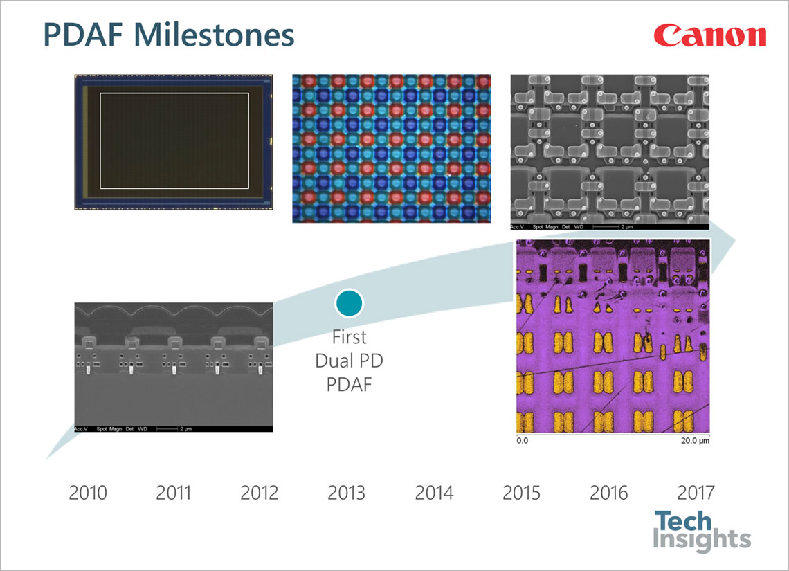
First Dual PD PDAF
D. Dual PD-Based Pixel PDAF
Given the lossy nature of a masked PDAF system, a second type of PDAF emerged in July 2013 when Canon announced its Dual CMOS AF system for the EOS 70D [12]. This new approach featured dual, front-illuminated PDs at each photosite (two PDs per pixel aperture/color filter). While all pixels featured the same dual PD structure, only the central ~80% were allocated to the AF system.
In March 2016 Samsung announced its back-illuminated dual PD system (Dual Pixel) developed for the Galaxy S7 smartphone [13]. These 1.4 µm generation dual PD pixels were available as AF points across 100% of the active pixel array. Variants of Samsung’s Dual Pixel technology were implemented both in Samsung and Sony-sourced chips in the Galaxy S7 [14,15]. In both versions, the PD pairs were isolated by partial-depth back DTI (B-DTI) structures to reduce crosstalk within the substrate. In addition to the conventional B-DTI structures used by the Sony variant, the Samsung version employed a 2x2 B-DTI sub-array for green and blue channel dual PDs.
The observed dual PD systems from Canon, Samsung and Sony use a standard Bayer-patterned RGB color filter array.
E. Dual PDAF
It is a reasonable assumption that both masked PDAF and dual-PD-based systems could exhibit degraded performance in low-light conditions. In the case of masked PDAF, the lower fill factor of partially-masked apertures results in photon loss, as compared to a non-masked neighbor. In the case of dual PD, the twin PDs would require isolation from one another and the surrounding structures. The additional isolation results in an overall reduced full well capacity, as compared to a single PD implemented in the same pixel size.
Recent back-illuminated Sony chips have been found to use a new type of PDAF system that could be described as lossless. The 1.0 µm pixel generation Exmor RS chip in the Apple iPhone 7 Plus used a 1x2 microlens structure over two of eight pixel pairs in selected green-blue rows [16]. The wide microlenses cover a green filter in the Bayer pattern and a green replacement filter in the neighboring blue position. Two of 64 pixels in an 8x8 block use this lens structure and these blocks are distributed across ~95% of the active pixel array. A similar implementation of 1x2 microlenses were found in use in the Sony IMX398 from the Oppo R9s and have been dubbed “Dual PDAF” [17].
| Chip Vendor | Year | Pixel Pitch (µm) | PDAF Pixel Configuration | Sensor Type/Configuration |
|---|---|---|---|---|
| Toshiba | 2010 | 1.6 | Half-mask | FI CCD |
| Aptina | 2011 | 3.4 | Half-mask | FI CMOS |
| Canon | 2012 | 4.3 | Variable-mask | FI CMOS |
| Canon | 2013 | 4.1 | Dual PD | FI CMOS |
| Toshiba | 2013 | 2.2 | Half-mask | BI CMOS |
| Sony | 2014 | 1.12 | Half-mask | Stacked, BI CMOS |
| Samsung | 2014 | 3.6 | Variable-mask | BI CMOS |
| Sony/Samsung | 2016 | 1.4 | Dual PD | Stacked, BI CMOS |
| Sony | 2016 | 1.0 | Dual PDAF | Stacked, BI CMOS |
Table 1. Noteworthy PDAF System Insertion Dates and Configurations
References
[1] FujiFilm press release, Jul. 21, 2010.
[2] “Fujifilm MS3961 Die Markings 12.0 MP, 1.6 μm Pixel Size CCD Image Sensor from Fujifilm FinePix Z800EXR Focused Technology Analysis (FTA) Report”, IPR-1009-801-01, -03, -04, -05, Oct. 2010.
[3] Nikon press release, Sep. 2011.
[4] “Aptina MT9J007C1HS 12 Megapixel (10.1 Megapixel Effective) CMOS Image Sensor with DR-Pix™ Technology from a Nikon V1 Camera Imager Process Review”, IPR-1110-804, Dec. 2011.
[5] Canon EOS 650D press release, Jun. 2012.
[6] “Canon LC1270 18.0 MP, 4.3 μm Pixel Size, APS-C Format CMOS Image Sensor from Canon EOS Rebel T4i (EOS 650D/EOS Kiss X6i)”, IPR-1206-802, Aug. 2012.
[7] “Sony IMX270, Micro Four Thirds, 20.4 MP Resolution, 3.3 µm Pixel Pitch, Front-Illuminated “Live MOS” CMOS Image Sensor from Olympus OM-D E-M1 Mark II MILC”, DEF-1703-802, Apr. 2017.
[8] Fujifilm press release, Jan. 2013.
[9] “Toshiba TCM5112CL CMOS Image Sensor from Fujifilm X20 Device Essentials Summary”, DEF-1311-803, Nov. 2013.
[10] “OmniVision OV16880, 1/3.06” Format, 16 MP Resolution, 1.0 μm Pixel Pitch Stacked (PureCel Plus-S) Back-Illuminated CMOS Image Sensor”, DEF-1606-804, Aug. 2016.
[11] Sony Xperia Z5 product page, Oct. 2015.
[12] Canon EOS 70D press release, Jul. 2013.
[13] Samsung press release, Mar. 2016.
[14] “Samsung S5K2L1, 1/2.6” Format, 12 MP Resolution, 1.4 μm Pixel Pitch Back-Illuminated Stacked ISOCELL CMOS Image Sensor from Samsung Galaxy S7 (Model SM-G930FD)”, DEF-1603-804, Apr. 2016.
[15] “Sony IMX260 12 MP, 1.4 μm Pixel Pitch Stacked BI CIS with DBI and Full Chip PDAF from the Samsung Galaxy S7 edge Rear-Facing Camera Imager Process Review”, IPR-1603-802, May 16, 2016.
[16] “Sony 12 MP Resolution, 1.0 μm Pixel Generation Stacked (Exmor RS) Back-Illuminated CMOS Image Sensor from iPhone 7 Plus Telephoto iSight Camera”, DEF-1612-801, Jan. 2017.
[17] Oppo R9s landing page, Oct. 2016.