Reducing Carbon Emissions will be a Challenge for Semiconductor Manufacturers
Author: Gibson Peters

The semiconductor industry has a problem when it comes to sustainable manufacturing processes and semiconductor emissions.
How do you continue to innovate and produce increasingly more powerful and complex silicon wafers, while simultaneously addressing environmental concerns related to the energy and water needs, as well as the chemical and carbon emissions that are part of the manufacturing process?
Platform Login Start My Free Trial
The manufacturing of semiconductors is energy intensive and uses a variety of high global Warming Potential (GWP) gases to create intricate circuitry patterns on silicon wafers. Reducing carbon from manufacturing is important because over 80% of the lifecycle carbon from Apple’s iPhone 14 Pro, Samsung‘s Galaxy S23, and Google’s Pixel 7 comes from the manufacturing stage. Most of these manufacturing emissions are the result of manufacturing advanced logic and memory semiconductors. As customers and AI applications demand more complex semiconductors, the demand for semiconductors will only grow.
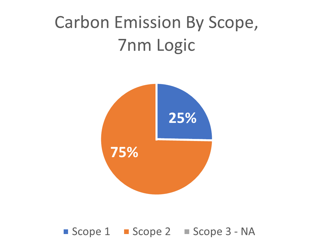
There are three major sources of semiconductor carbon emissions associated with the manufacturing of chips: emissions from process gases, natural gas burned on-site, and emissions associated with electricity used. These emissions are generally classified into two categories Scope 1 and Scope 2 emissions (Figure 1). Scope 1 emissions are direct greenhouse gas emissions occurring from sources that are controlled or owned by an organization. Scope 2 emissions are indirect emissions associated with the purchase of electricity. For example, if a company purchases electricity from a coal plant, that electricity will have a higher carbon intensity (CO2e/kWh) than if the same facility purchases electricity from a wind farm.
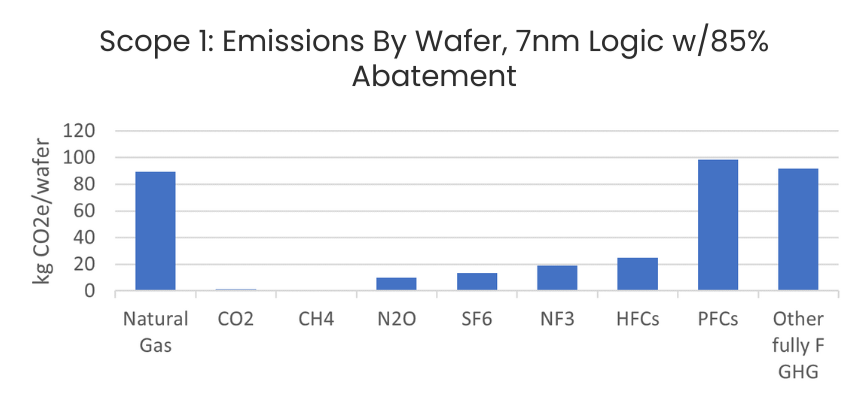
Large fabs can use as much as 100 megawatt-hours of power each hour—more than many oil refineries and automotive plants. Semiconductor manufacturing uses not only large quantities of electricity but also some of the most greenhouse-intensive gases in the world like SF6, with GWP 23,500, and NF3, with GWP 16,100, in their manufacturing processes. GWP 23,500 means 1 ton of SF6 released into the atmosphere has the same GWP as 23,500 tons of carbon dioxide (CO2). Luckily there is abatement technology that can capture up to 99% of process chemicals, but small emissions of process gases can lead to large carbon emissions. Even with good abatement equipment installed at a Scope 1 facility, emissions can be significant. Figure 1 shows the ratio of Scope 1 versus Scope 2 emissions for a 7nm logic integrated circuit (IC), and Figure 2 shows a breakdown of Scope 1 emissions by wafer for the same IC. Emissions change significantly based on location, processes used to manufacture, and abatement technologies used at the facility.
Semiconductor manufacturing is extremely complex, and companies invest billions into building facilities to manufacture facilities and years of fine-tuning processes. One of the big challenges facing semiconductor manufacturing is maintaining manufacturing precision and yield. Companies are reluctant to introduce new equipment and processes that might impact yield and profitability. We must start somewhere and identify the best opportunities to reduce carbon from semiconductor manufacturing.
Figure 1
TechInsights’ mission is to identify and highlight processes and equipment with high electricity use and process gas emissions so our customers have the sustainability tools to report, compare, and reduce carbon emissions.
Figure 2
Watch this space, and in my next report we will take a look at three primary opportunities semiconductor manufacturers have to reduce their emissions.


