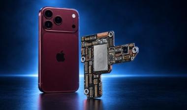
Apple A20 Pro Analysis
Apple A20 Pro: Inside the iPhone 18 Pro’s TSMC 2nm Processor
TechInsights reveals how Apple and TSMC are bringing 2nm gate-all-around technology, expanded AI processing, and advanced memory packaging to the iPhone 18 Pro.
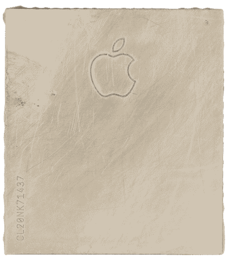
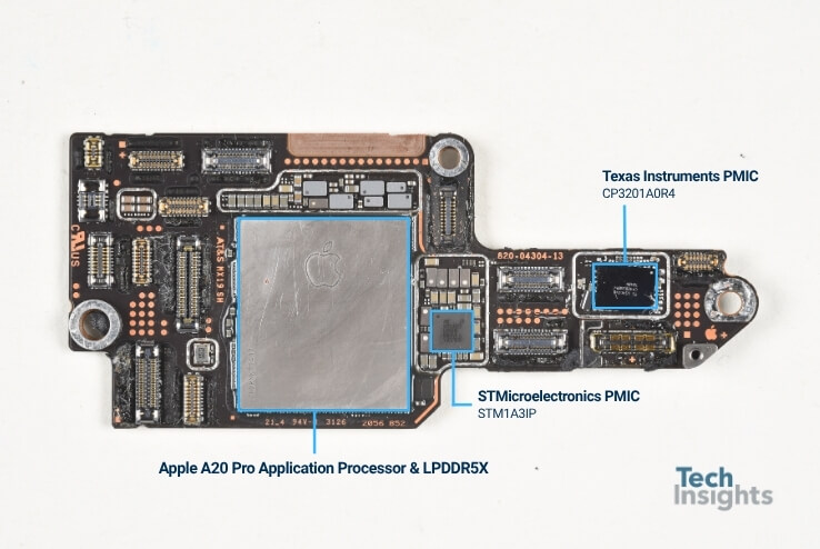
Apple’s A20 Pro represents an important transition for mobile semiconductor technology. Extracted from the iPhone 18 Pro, the processor is the first Apple application processor manufactured using TSMC’s N2 process, introducing gate-all-around transistors to the iPhone platform.
TechInsights is now analyzing the A20 Pro package, compute die, process architecture, functional blocks, and memory configuration to determine how Apple and TSMC have implemented this first-generation 2nm technology.
Key Findings
- Transistor architecture and critical dimensions
- Logic-cell scaling and estimated gate density
- SRAM-cell and cache scaling
- Process variability and manufacturing execution
- Die floorplan and functional block allocation
- CPU, GPU, and neural processing architecture
- Package construction and memory integration
- Comparisons with TSMC N3, Samsung SF2, and Intel 18A
Why TSMC N2 Matters
TSMC N2 marks the foundry’s transition from FinFET transistors to a gate-all-around architecture.
In a gate-all-around transistor, the gate surrounds stacked nanosheet channels on all four sides. This provides greater electrostatic control than a conventional FinFET structure, helping reduce leakage while improving performance and energy efficiency.
For the A20 Pro, these characteristics are particularly important. Mobile processors must deliver greater compute performance while operating within strict battery, temperature, and device-size constraints.
TechInsights’ exploratory analysis indicates that the A20 Pro uses aggressively scaled logic cells enabled by TSMC’s nanosheet architecture. The complete report examines how this process-gate density-scaling compares with TSMC’s previous N3 technologies and competing 2nm-class processes from Intel and Samsung.
More Graphics and AI in a Similar Die Area
The A20 Pro compute die measures approximately 8.0 mm by 12.3 mm, producing an estimated die area of 98.2 mm². This is nearly identical in size to the previous-generation A19 Pro.
Despite the similar die area, the A20 Pro appears to contain an additional GPU core and significantly more space dedicated to neural processing.
Preliminary floorplan analysis confirms a six-core CPU configuration with two performance cores and four efficiency cores. Each performance core appears to have access to dedicated L2 cache, while the efficiency cores share cache across multiple banks.
The expanded neural processing area includes neural compute engines designed for matrix multiplication and convolution operations used in machine learning and on-device AI workloads.
This increased allocation to graphics and AI suggests that Apple is using the density and efficiency benefits of N2 to add functionality rather than simply reduce die size.
Exclusive webinar · Apple iPhone 18
Go inside Apple’s newest Pro iPhones.
Discover what preliminary teardown evidence reveals about Apple’s A20 Pro processor, camera and connectivity systems, component suppliers, packaging, and device cost. Join TechInsights experts for an evidence-based look beyond the Apple announcement.
Register for the Webinar →A New Packaging and Memory Architecture
The A20 Pro also introduces an important packaging change.
Apple has moved away from the traditional package-on-package approach, where memory is positioned directly above the processor. In the new architecture, the processor and memory are positioned side by side within a wafer-level multi-chip module.
This arrangement may improve heat transfer while enabling a wider memory interface. Preliminary analysis points to a 96-bit LPDDR5X interface designed to deliver the additional bandwidth required by graphics and on-device AI workloads.
The full TechInsights analysis will examine how this packaging approach affects signal routing, thermal performance, package construction, and memory integration.
How Does TSMC N2 Compare?
TSMC is not the first foundry to introduce a 2nm-class gate-all-around process. Intel and Samsung have already moved to related transistor architectures, but their implementations differ.
Intel 18A combines its RibbonFET gate-all-around transistor with backside power delivery. Samsung SF2 and TSMC N2 retain front-side power delivery, which may make it easier for designers to adapt existing system-on-chip architectures.
TechInsights’ early observations also identify structural differences between the TSMC and Samsung implementations, including the integration of inner spacers within TSMC’s nanosheet transistor architecture.
These process choices can affect performance, leakage, density, manufacturing complexity, and long-term scalability.
Stay Ahead of the Rest
Access the Complete A20 Pro Analysis
The complete TechInsights report provides detailed package, die, floorplan, and process analysis of the Apple A20 Pro, including early measurements and comparisons with other leading-edge semiconductor technologies.
This analysis is available on the TechInsights Platform. Register or log in to explore the findings and follow the report as additional reverse-engineering results are released.
Registered on the TechInsights Platform? Receive the latest iPhone 18 teardown findings, reverse-engineering analysis, and expert insights. Once registered, click Follow the analysis to be notified as soon as new analysis is released.