Apple iPhone 6s Teardown
Posted: September 25, 2015
Contributing Authors: Dick James, Daniel Yang, Stacy Wegner, Chad Davis & Albert Cowsky
It’s now a yearly ritual - go line up and get the new iPhone! This year Apple did multi-country launches, and allowed pre-orders to be picked up from the store, so no more driving down to the US and queuing for hours to be sure of getting one or two.
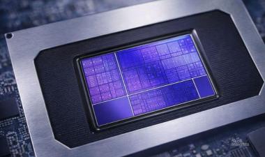
Our local Apple outlet opened at 8 am, so by 8.30 we had it in the lab and started the dismantling - the first order of priority is to get the new A9 chip off the board, decapsulated and then cross-sectioned to see who made it, and whether it’s made with the 14/16 nm finFET process that everyone in the tech media is expecting.
Register for a complementary product report.
Apple iPhone 6s Promotion
What's in the A9?
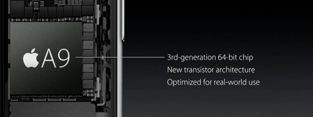
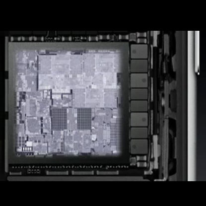
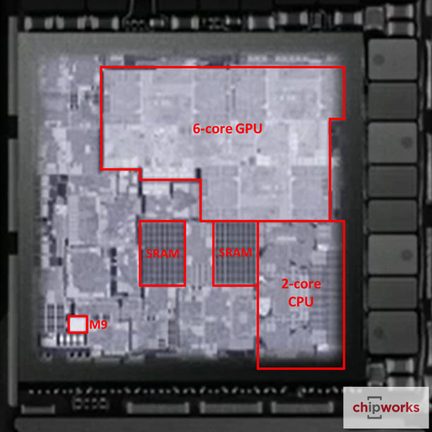
During the launch event Apple told us there would be a “new transistor architecture” in the A9, which does sound like a euphemism for a switch to finFET (first image below). They also showed what looked like a die layout of the A9 - here’s a screen shot in the first thumbnail image below. With something as teasing as this, we couldn’t resist comparing it with the A8 (second thumbnail). In the A9, it looks like we have two blocks of SRAM in the lower centre, a dual-core CPU at the lower right, and possibly a six-core GPU at the upper right. And of course the M9 motion coprocessor is now apparently integrated onto the chip. That gives us the following view (see last thumbnail).
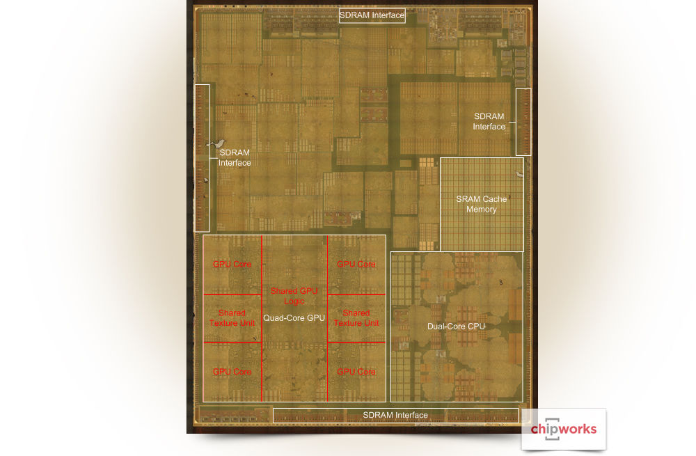
Apple iPhone 6s Die Photo
If one of those SRAM blocks is 4 MB, then we can take a guess as to the die size. In the A8 that block was ~4.9 mm2, so with a 80% linear shrink (64% area shrink) it would be ~3.1 mm2, or with a 70% shrink it would be ~2.4 mm2. If we compare the block size with the whole die, that gives us respective die sizes of ~93 mm2 or ~71 mm2, although given the fuzzy edges in the image, there is room for error in those numbers (the A8 was ~89 mm2).
Those die sizes seem to be in Apple’s preferred range in the earlier iPhones, so that gives us the assumption that there is now 8 MB L3 cache, up from the 4 MB in the A8. Comparison of SRAM areas in the CPU with our reference block also indicates there may be 3 MB of shared L2 cache in there.
Apple iPhone 6s Teardown
Everything else is changed?
Other updates that we’re going to look at include the new cameras, the expanded RF frontend (since the new phone has more worldwide connection capability than the last one), the new display and 3D Touch screen controllers, and of course we want to know who won the sensor and power management design slots. We know that there is a new fingerprint sensor in there, and the display controller now uses the backlight as a flash for selfies.
In the last few phones Apple has gone for pretty decent cameras, to the extent that movies have been made on iPhones; and it looks like the new one is no exception, it was a big part of the sales pitch on the 9th September. It’s not often that “deep trench isolation” gets mentioned in such events, but with our expertise in image sensors we know that this is leading-edge technology, and we’ll be doing serious analysis on the new camera chip.
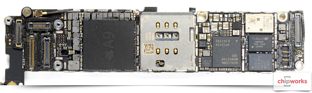
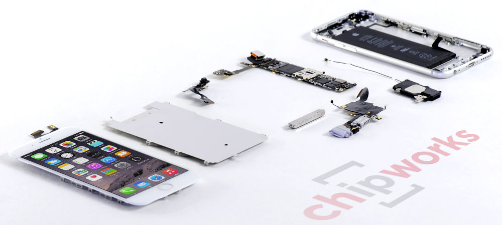
Apple iPhone 6s Board Shot Front
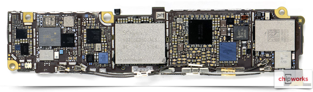
Apple iPhone 6s Board Shot Back
What have we found?
First off - Apple’s new A9 processor is the APL0898, and it’s ~8.7 x 10.7 mm, or ~94 mm2, which agrees with our 80% shrink guesstimates. Maybe that’s a reflection of the 14/16 nm processes only shrinking the transistor dimensions, not the metallization, maybe it means that Apple have crammed more in there (probably both). And it seems to confirm our postulated 8MB of L3 cache.
Now let's do inventory
- 3 x Knowles KSM2 microphones
- 2 x Apple/Cirrus Logic 338S1285 Audio IC (likely an iteration of the 338S1202 audio codec found in the iPhone 5s)
- Apple 343S00014 3D Touch Controller?
- Apple A9 APL0898 application processor
- Apple/Cirrus Logic 338S00105 Audio IC
- Apple/Dialog 338S00120 Power Management IC
- Avago ACPM 7714 Multimode Power Amplifier
- Avago AFEM-8030 Power Amplifier Module
- Bosch Sensortec 367 LA 3-axis Accelerometer (likely BMA280)
- Bosch Sensortec barometric pressure sensor BMP280 ?
- Goertek GWM1 microphone
- InvenSense MP67B 6-axis Gyroscope and Accelerometer Combo (also found in iPhone 6)
- Micron D9SND (MT53B256M64D2NL) 2 GB LPDDR4 SDRAM
- Murata 240 Front-End Module
- Murata(?) Ne G98 RF Front-End Module
- Murata(?) Yd G54 RF Front-End Module
- NXP 1610A3 (likely an iteration of the 1610A1 found in the iPhone 5s and 5c)
- NXP 66V10 NFC Controller (vs. 65V10 found in iPhone 6)
- Qorvo/RFMD RF1347 Antenna Switch Module
- Qorvo/TriQuint TQF6405 Power Amplifier Module
- Qualcomm MDM9635M LTE Cat. 6 Modem (vs. the MDM9625M found in the iPhone 6)
- Qualcomm PMD9635 Power Management IC
- Qualcomm QFE1100 Envelope Tracking IC
- Qualcomm WTR3925 Radio Frequency Transceiver
- RF Micro Devices RF5150 Antenna Switch
- SK Hynix H23QDG8UD1ACS Dual Die Package (DDP) 64Gb NAND Flash
- Skyworks SKY77357 Power Amplifier Module (likely an iteration of the SKY77354)
- Skyworks SKY77812 Power Amplifier Module
- Texas Instruments 3539 LED backlight Retina display driver
- Texas Instruments 65730AOP Power Management IC
- Texas Instruments 6BB27
- Texas Instruments SN2400AB0 Charger IC retained from the iPhone 6
- Universal Scientific Industrial 339S00043 Wi-Fi Module
Apple iPhone 6s Bill of Materials Cost
Apple iPhone 6s Bill of Materials Cost
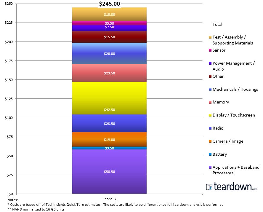
The bill of materials cost for Apple's A1688 64 GB iPhone 6s is estimated to be $245.00.
The major components that make up this cost are the applications + baseband processor, display subsystem, and memory. The iPhone 6s we analyzed is the 64 GB version however we have normalized costs to 16GB for ease of comparison. The following chart illustrates the breakout of costs by major component.
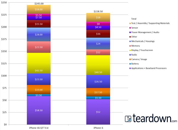
Apple iPhone 6s vs Apple iPhone 6 Cost
Quick Comparison of iPhone 6 versus iPhone 6s
The following chart compares the iPhone 6 and the iPhone 6s QTT estimated bill of materials costs. The iPhone 6 bill of material costs are from our released Deep Dive report, rounded to the nearest $0.50 to help with comparing to our quick turn estimates for the iPhone 6s QTT. In general for our QTTs, our estimates are rounded to the nearest $0.50.
There were some significant increases in costs for the iPhone 6s. The move to a 2GB LPDDR4 memory IC caused the greatest impact for the memory cost; our 2GB LPDDR4 accounts for $16, versus the $4.50 1GB LPDDR3 in the iPhone 6.
- The redesign of the aluminum enclosure using 7000 series impacted the Mechanical/Housing cost by an estimated $4. We will take a closer look at during our deep dive to see if there are other fabrication techniques in the iPhone 6s versus the iPhone 6.
- The display increase was due to the 3D Touch Sensor and its touch controller IC.
- As for the lower cost of for the Radio – this was QTT estimate based solely on what we could verify. We did find there to be suspicious ICs which could be a part of the radio - this will be confirmed in our final report.
- The increase in camera costs: the iPhone 6s now has a 5 MP front camera and a 12 MP main camera – both are upgrades from the iPhone 6.
- The Apps + Baseband: The introduction of the A9 processor with the M9 designed into it increased the cost from the iPhone 6 which had an A8 and a separate M8 processor.
- Another consideration was the Baseband processor costs. The iPhone 6s uses a new Qualcomm part, the MDM9635M whereas the iPhone 6 had the MDM9625M.
What have we learned?
The APL0898 size fits with an 80% shrink on the A8, and seems to have 8 MB cache - and our first look leads us to believe that our sample is from Samsung.
For the first time we have seen, Micron has put some memory into the iPhone (though iFixit’s sample has Samsung), and it’s up to 2 GB for the first time for an Apple phone. As expected, they are dual-sourcing (at least) the flash - we have Hynix, iFixit has Toshiba.
Sensors
When it comes to the sensors, we have the same Invensense/Bosch motion sensor duopoly that we had in the iPhone 6/6 Plus. Goertek has maintained its mircrophone slot whereas AAC has lost its place to Knowles.
Wireless
The wireless part of the phone is again dominated by the Murata/Avago/Qorvo tripoly (Qorvo is the new name for the Triquint/RF Micro Devices merger) for the RF front end, and at least in this part of the world, Qualcomm has the broadband sockets.
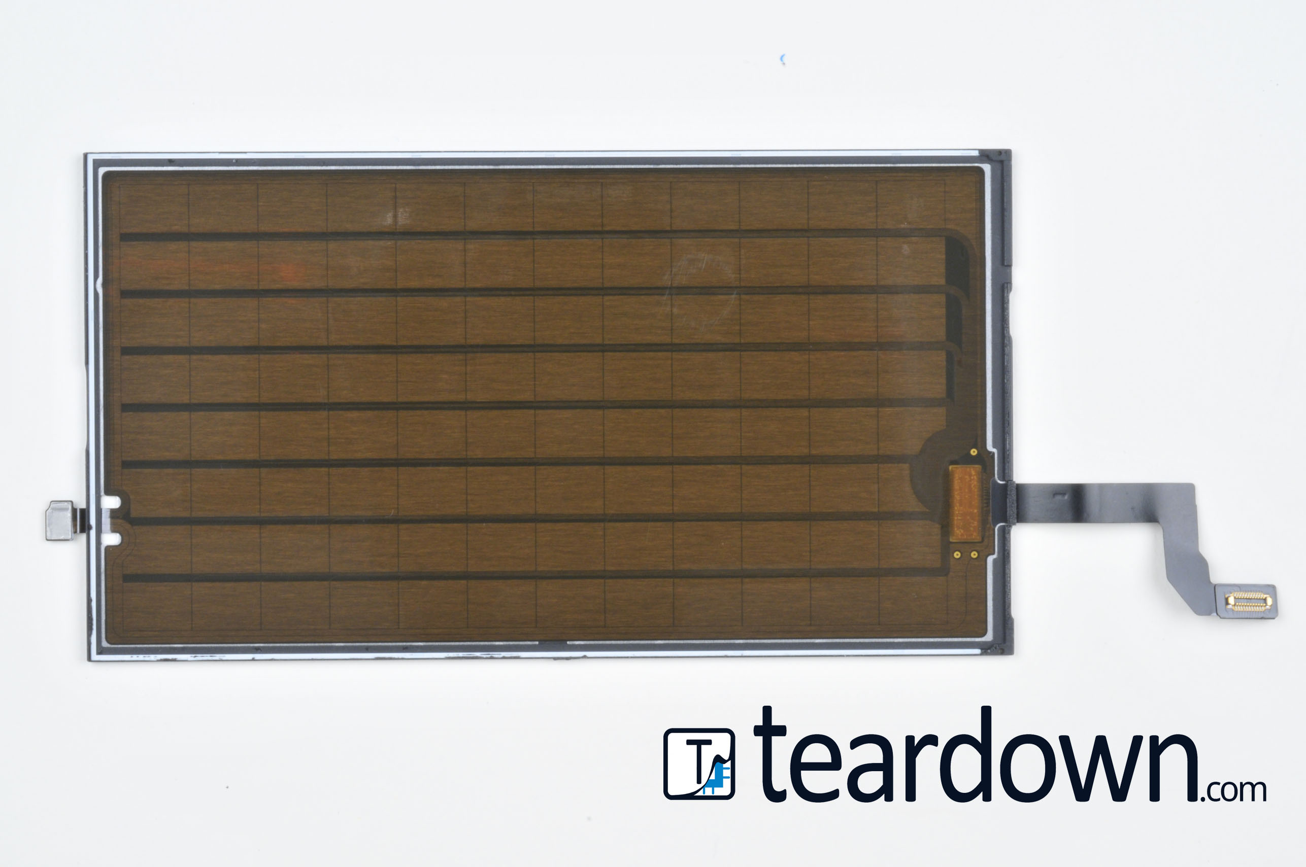
3D Touch screen
3D Touch screen
The team at teardown.com has identified the 3D Touch capacitive touch sensor (first image) and controller (second image) behind Apple's 3D Touch display.
3D Touch appears to be what Apple’s marketing department is most excited about. With 3D Touch, the screen becomes pressure sensitive. Upon release, the company’s website was full of demos of 3D Touch technology, stressing how the feature would allow users to move through apps, email, messages and the internet more seamlessly.
Apple touts the ability to “Peek and Pop” on the iPhone 6s. Say a user receives a link in a message: With a hard press, users can “Peek” at the webpage being linked to by bringing up a preview. With a deeper press, they can “Pop” into the full webpage. A few other use cases consumers are bound to love? Hard press the keyboard to turn it into a cursor, or hard press a photo to see a second of movement before and after the photo was taken.
The only other OEM promoting Force Touch at present is Huawei. The Huawei Mate S is slated to be released in late 2015.
As an aside, we tore apart the Blackberry Storm 9500 way back in 2009. If you remember, it too featured a patented capacitive touchscreen . However, the novelty might have been lost on consumers six years ago because there certainly weren’t as many engaging ways to use it. Interesting how far we have — or haven’t — come.
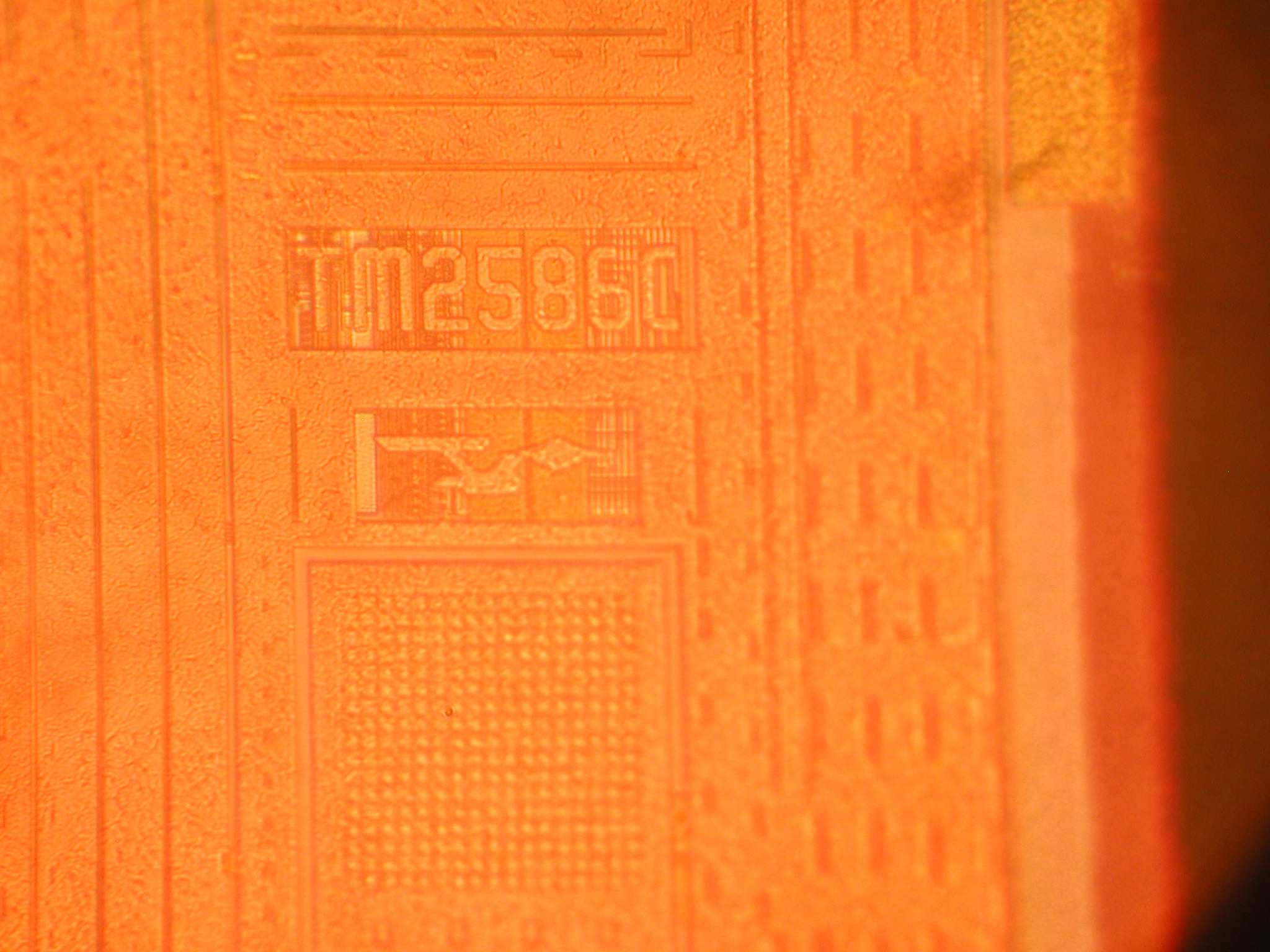
AMS Ambient Light sensor die photo
AMS Ambient Light Sensor
The U.S.S. Enterprise has been located inside the Apple iPhone 6s (AMS Ambient Light sensor die photo)
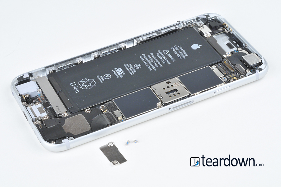
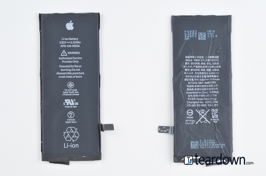
Apple iPhone 6s Battery
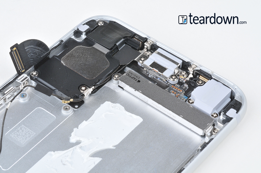
Battery
Unmissable above the Taptic Engine is the battery pack. It’s hard to discern visually, but the 6s battery is slightly smaller in capacity than its predecessor. The current Li-ion battery is rated at 3.82V and 6.55Whr. Apple took a dip in Milliamp hours, decreasing them from 1810 mAh in the iPhone 6 to the current 1715 mAh.
The drop in overall charge capacity shouldn't impact running time thanks to the efficient A9 processor and embedded M9 motion coprocessor. Apple claims battery life will deliver 14 hours of talk-time and 10 days of standby. This is the same as claimed by the iPhone 6.
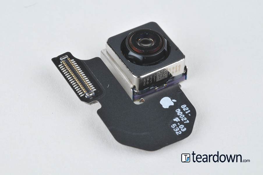
Camera
Camera
The iPhone 6s camera features a 12-megapixel rear-facing camera — the most megapixels on an iPhone yet. Apple uses trench isolation to prevent leakage between photodiodes, yielding crisp, clear photos. Apple also upgraded the front-facing camera to 5-megapixels.
We will spend a fair bit of time on this device. A detailed analysis of the image sensors and technology updates will be available in our full report.
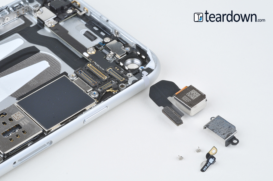
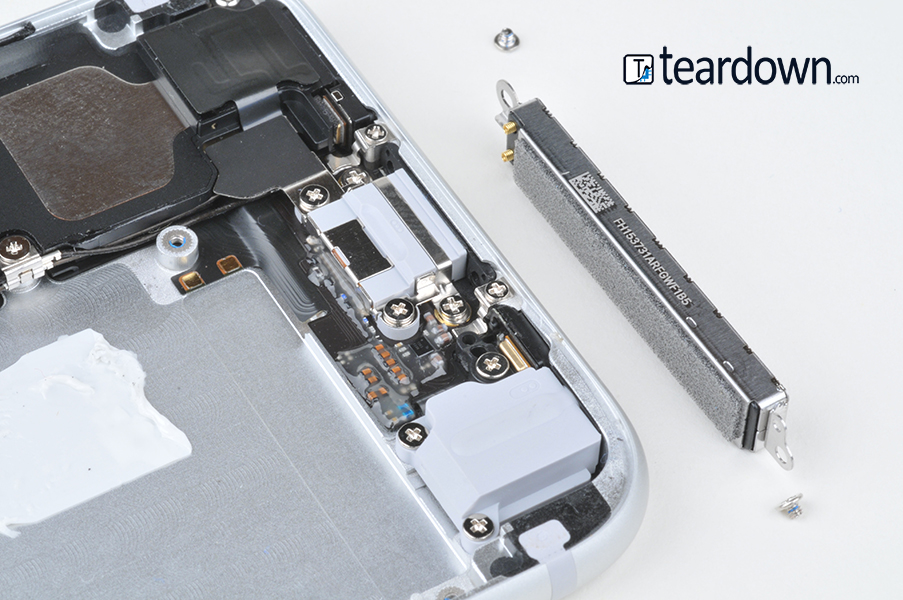
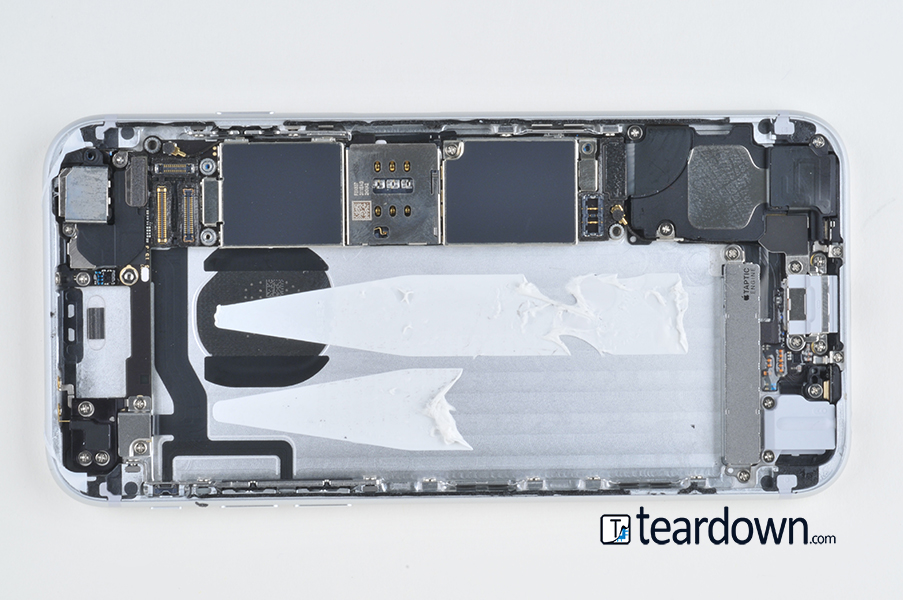
Apple Taptic Engine
The Taptic Engine
The world was first introduced to Apple’s Taptic Engine by the Apple Watch. On the smartwatch, the feature gives “real-time feedback” to the wearer through subtle taps on the wrist. When living within an iPhone, the Taptic Engine resides inside aluminum casing just below the battery (more on that later), taking the place of the previous vibrator.
The Taptic Engine is an integral addition to the iPhone 6s, as it’s what gives the fast-as-lightning haptic feedback in response to the 3D Touch display. Wherever a user presses deeply, for example, the oscillating mechanism will fire up in one cycle — quicker than the standard vibrator. In short: Less power consumption, more kinetic energy. It’s worth noting that the iPhone 6 vibrator also featured linear oscillation.
It’s certainly not lost on us that the introduction of the Taptic Engine in phone-form is a great way to inspire developers to create apps that incorporate it. Just think about the possibilities when it comes to gaming.
This is a larger version of the Apple Taptic Engine found in the Apple Watch.
The inclusion of the Taptic Engine at the expense of battery space is likely to meet the need to increased feedback from Apple's 3D Touch and the need for a wider variety of motion to be generated based on user activity.
We would expect the inclusion of the Taptic Engine to be of interest to appdevelopers who will be able to create more customized feedback for their applications and games.
The markings found on the Taptic Engine are FH153731ARFGWF1B5.
Aleady a subscriber?
TechInsights Teardown subscribers already have access to exclusive content in the TechInsights Platform.
Interested in a subscription?
TechInsights offers subscriptions to the broadest range of analysis and expert commentary. Contact us to learn about our many subscription offerings.