AMD Ryzen 7 9800X3D Processor Floorplan Analysis

Deep dive into the AMD Ryzen 7 9800X3D teardown—exploring components, die utilization, critical dimensions, and manufacturing costs for expert insights.
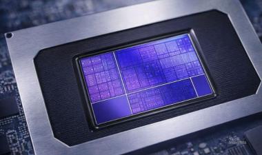
The AMD Ryzen 7 9800X3D 100-000001084 desktop processor is stacked L3 cache SRAM, compute chiplets along with a larger I/O chiplet located under the heat spreader and all three chiplets are manufactured by TSMC. This report analyzes the compute chiplet with "AMD ©2022 ELCCD" die markings. The AMD ELCCD die was fabricated on 300 mm wafers by TSMC, using the 4 nm (N4X) FinFET high-k metal gate (HKMG) CMOS process. N4X is TSMC's first process optimized for high performance computing (HPC). It has eight Zen 5 Cores and 32 1MB L3 cache memory blocks. This analysis includes node identification, BELO stack, bit cell usage, critical dimensions, and digital blocks layout with die utilization calculations for total area for logic, I/O memory, and analog components separately. Manufacturing cost is also provided.


