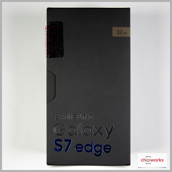
Posted: April 24, 2016
Contributing Authors: Jim Morrison, Ray Fontaine, Dick James and Daniel Yang
The following teardown blog contains some of our initial findings. For more in depth information on these topics and more, download the full Galaxy S7 edge teardown report.
Register for a complementary cost estimate.
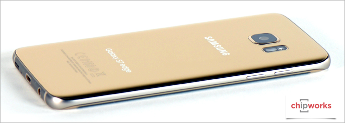
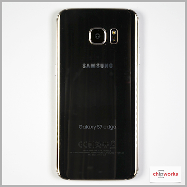
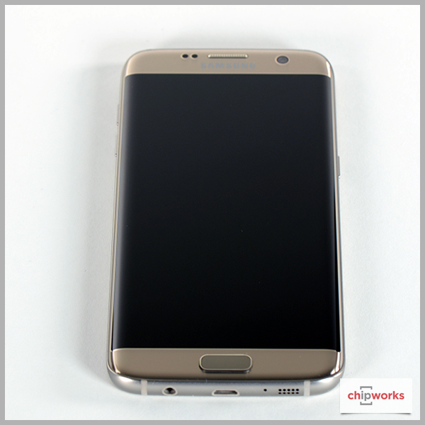
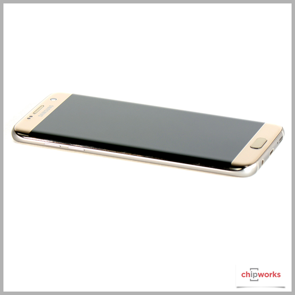
Samsung Galaxy S7 Edge
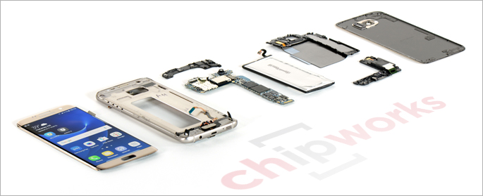
The rumors of shipments by T-Mobile of the new S7 and S7 Edge are true. We were among the fortunate few who received our units today. Teardown days at Chipworks are very fun. We are always looking forward to iPhone and Galaxy days especially. Everyone is eager and wants to chip in so they can be the first ones inside the technology. It’s very exciting.
We are expecting many new devices inside the S7 and S7 Edge, so this blog will probably be spread over a few days. We will be deprocessing many of the chips and this takes time. Immediately, it’s the display that grabs you. It is a stunningly brilliant AMOLED display with a resolution of 1440 x 2560.
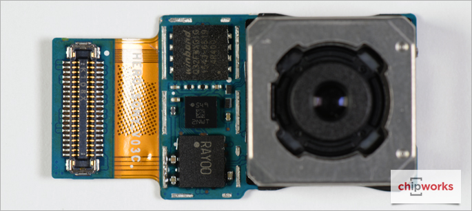
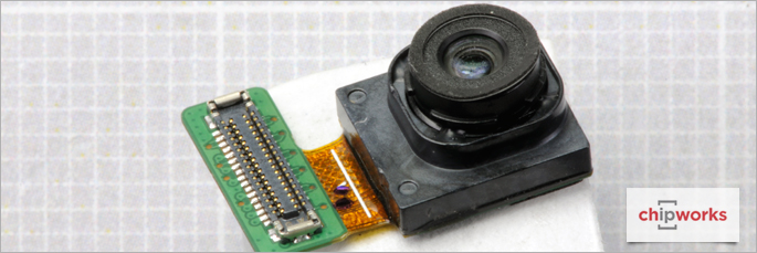
12 MP Rear-Facing Camera with Dual Pixel Autofocus (AF)
12 MP Rear-Facing Camera with Dual Pixel Autofocus (AF)
Just as Apple had, in 2013, reversed the pixel shrink trend of the time by transitioning from a 1.4 µm to 1.5 µm pixel pitch (iPhone 5 and 5s respectively), Samsung has similarly increased the pixel pitch of the Galaxy S7’s rear-facing camera. While the S6’s 16 MP camera featured 1.12 µm pitch pixels, the S7’s rear-facing camera now uses 1.4 µm generation pixels. Apple has since settled in on a 12 MP resolution (currently with a 1.22 µm pixel pitch) for the iPhone 6s/6s Plus cameras. Samsung now meets Apple head-to-head at the 12 MP resolution with its larger pixels. We’ll have to wait and see who wins the image quality battle; as of now, DxOMark Mobile does not have a score for the S7/S7 Edge. Currently tied for 1st place are Sony’s Xperia Z5 camera, which features a 23 MP sensor with 1.12 µm pitch pixels, and the 16 MP Samsung Galaxy S6 Edge Plus camera.
Just as Apple had, in 2013, reversed the pixel shrink trend of the time by transitioning from a 1.4 µm to 1.5 µm pixel pitch (iPhone 5 and 5s respectively), Samsung has similarly increased the pixel pitch of the Galaxy S7’s rear-facing camera. While the S6’s 16 MP camera featured 1.12 µm pitch pixels, the S7’s rear-facing camera now uses 1.4 µm generation pixels. Apple has since settled in on a 12 MP resolution (currently with a 1.22 µm pixel pitch) for the iPhone 6s/6s Plus cameras. Samsung now meets Apple head-to-head at the 12 MP resolution with its larger pixels. We’ll have to wait and see who wins the image quality battle; as of now, DxOMark Mobile does not have a score for the S7/S7 Edge. Currently tied for 1st place are Sony’s Xperia Z5 camera, which features a 23 MP sensor with 1.12 µm pitch pixels, and the 16 MP Samsung Galaxy S6 Edge Plus camera.
So what is new with the S7’s camera system? Dual pixel phase detection autofocus (PDAF) technology! We first saw this concept in use in 2013 in a much different imaging application: the Canon EOS 70D DSLR. Canon committed 80% of the 70D’s active pixel array to dual pixel CMOS AF functionality. A similar concept has now been adapted to the world of small-pixel mobile camera chips, where 100% of the 12 MP active pixel array is committed to both sensing and providing data to the AF system. What is impressive about the new dual pixel feature is the chip design team's ability to roll out this technology in a 1.4 µm pixel generation (Canon’s DSLR system used 4.1 µm generation pixels). The results are stunning – the S7’s photos are of high quality, especially when viewed on its Quad HD display. We haven’t seen a claim for the S7’s AF system speed yet. As a reference point, Sony has reported a 0.03-second focus speed for its hybrid (contrast and phase detection) AF system in the Xperia Z5.
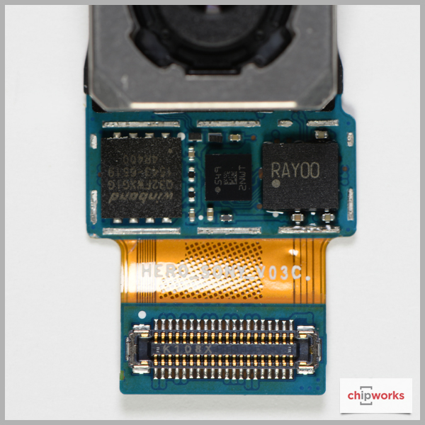
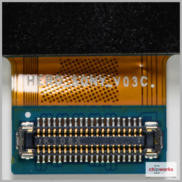
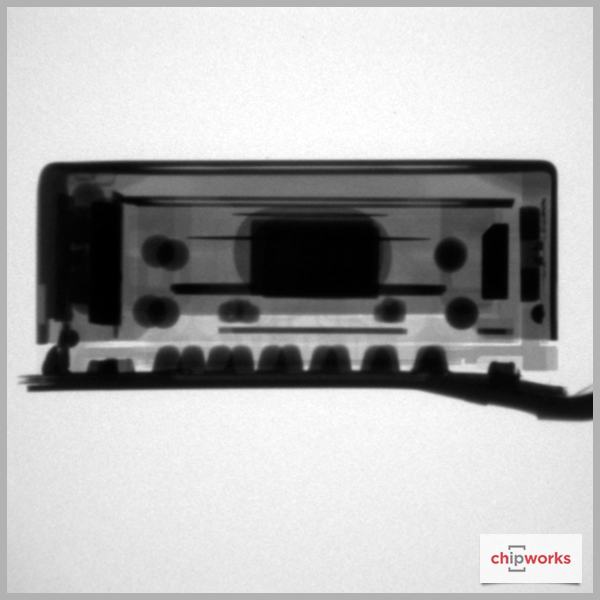
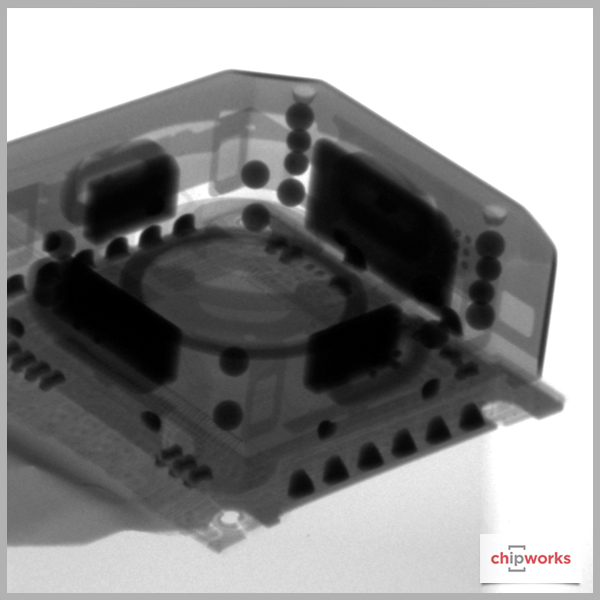
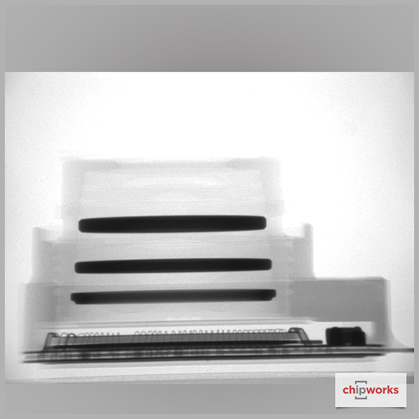
We’ll be doing more thorough analysis of the dual pixel technology over the coming days and weeks, but our initial review of the 12 MP camera module shows a camera module size of 12.1 mm x 12.1 mm x 5.4 mm thick. We’ve been reading the web articles indicating a Sony IMX260 design win for the 12 MP socket and we’re eagerly awaiting results from our lab to confirm. Based on the “SONY” logo on the module’s flex cable, we believe the speculation to be true.
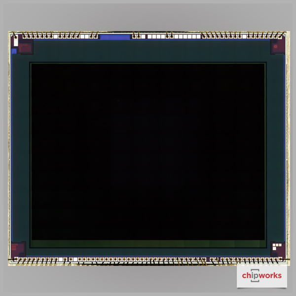
Rear-Facing Camera Die Photo
Rear-Facing Camera Update #1
Our lab staff have removed the imaging chip from the 12 MP camera module and have found a Sony back-illuminated (Exmor R) CMOS image sensor. We were expecting to find TSV arrays around the periphery of the active pixel array, corresponding to Sony’s stacked chip (Exmor RS) technology platform. Sony hasn’t publicly announced the IMX260, but based on what we’ve been reading, we assume that is the part number. It’s a bit of a surprise that the IMX260 isn’t an Exmor RS sensor, as we’ve been documenting a lot of Sony design wins based on its 1st and 2nd generation Exmor RS technology. It seems the full chip PDAF functionality, which requires dual readout from each pixel, was implemented with a multi-chip solution rather than a stacked (CIS + ISP) solution.
The Sony IMX260 die size, as measured from the die seals, is 6.69 mm x 5.55 mm (37.1 mm2). There are no conventional die identification markings in use on the die, consistent with back-illuminated (stacked/non-stacked) Sony CIS chips. We confirmed a pixel pitch of 1.4 µm and a Bayer-patterned color filter array. Work on this chip is ongoing and we will be reporting on this small-pixel event more extensively with a Device Essentials project and through our Image Sensor subscription service.
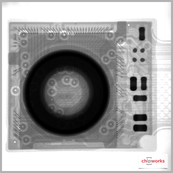
Rear-Facing Camera
Rear-Facing Camera Update #2
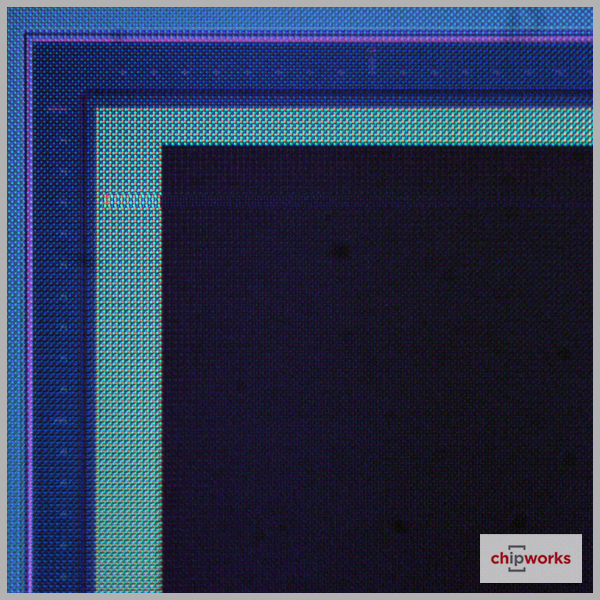
Our lab staff have completed the initial cross-sectioning work for our IMX260 project and we have a substantial update to share: the Sony IMX260 is, in fact, a stacked chip CMOS image sensor! As mentioned, we had expected to find through silicon vias (TSVs) consistent with Sony’s Exmor RS technology platform. Our early teardown results revealed what appeared to be a conventional Sony non-stacked back-illuminated (Exmor R) chip. After going deeper inside, we see that Sony is leading the digital imaging sector into an era of hybrid bonding. It’s not currently known if Sony considers this an extension of its Exmor RS platform, or if the IMX260 marks the first of a new (as of now unannounced) family of back-illuminated image sensors. For now we consider the IMX260 to be a 3rd generation Exmor RS chip.
Sony has previously announced a licensing relationship with Ziptronix (now owned by Tessera) for wafer bonding technology. Sony licensed ZiBond® technology in 2011 and expanded the relationship in 2015 by licensing direct bond interconnect (DBI®) hybrid bonding. We didn’t expect to find it in use in the Galaxy S7 as Sony typically promotes such technological evolutions with a press release and/or product announcement. Regardless, that’s why we do the teardowns – to see what’s actually inside technology!
Our cross-section reveals a 5 metal (Cu) CMOS image sensor (CIS) die and a 7 metal (6 Cu + 1 Al) image signal processor (ISP) die. The Cu-Cu vias are 3.0 µm wide and have a 14 µm pitch in the peripheral regions. In the active pixel array they are also 3.0 µm wide, but have a pitch of 6.0 µm. Note that in the images we’ve included we do see connections from the Cu-Cu via pads to both CIS and ISP landing pads. The Cu-Cu vias in the active pixel array don’t appear to have connections to either the CIS or ISP so they may be included for via uniformity, however these are preliminary results and we plan on additional cross-sectional and planar analysis to provide full coverage of the IMX260’s interconnections.
The successful rollout of wafer-to-wafer direct bonding has broader implications for the general semiconductor industry, but it’s especially important to the image sensor community. We’ve been seeing this technology in literature for a few years now, but the IMX260 represents the first known direct bond interconnected chip to be used in a such a high volume consumer application as the Samsung Galaxy S7 camera. That’s it for today’s update - we wanted to share these new images as soon as possible. There is much more to the story and as our analysis continues we’ll summarize this new state-of-the-art in our upcoming reports.
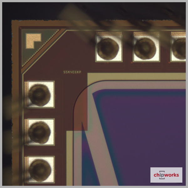
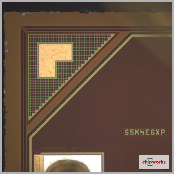
5 MP Front-Facing Camera
5 MP Front-Facing Camera
The front-facing camera module size is 8.0 mm x 7.2 mm x 5.0 mm thick. It contains a back-illuminated Samsung die with S5K4E6XP die markings. The chip has a confirmed pixel pitch of 1.34 µm and uses a Bayer-patterned color filter array.
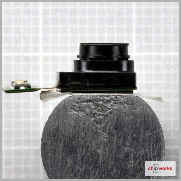
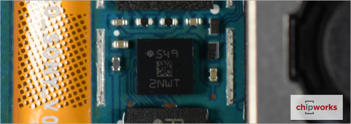
Optical Image Stabilization Inertial Sensor
Optical Image Stabilization Inertial Sensor
On the flex tail coming off of the primary camera module, we find an STMicroelectronics K2G2IS gyroscope for image stabilization.
Design Wins
As soon as we got the cover off, we were able to start to ID some parts. For example, some of the the sensors and wireless chips are in plain view:
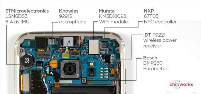
Design Wins
Once we got the motherboard out, we wanted to go straight for the application processor to look at the much-vaunted Qualcomm Snapdragon 820, but of course it is hidden under the Hynix LPDDR4 SDRAM in a package-on-package (PoP) format, as in almost all smartphones.
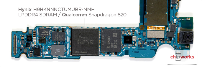
Application Processor
However, we are adept at popping off the top part of the PoP, so it didn’t take long to find the Snapdragon 820, now confirmed as the MSM8996. We’ll have to wait until the chip is off the motherboard and decapsulated before we can look at the die itself. We might have to wait to look at it, but if you’re interested in its capability, our friends over at AnandTech reviewed the performance of the 820 at the end of last year.
MSM8996
One thing we noticed is the large increase in the interconnecting solder bumps between the top and bottom parts of the PoP – earlier generations had only two rows connecting the two parts. This could be a result of the higher memory bandwidth being used these days, and/or the need to dissipate more heat from the higher performing processor, particularly the GPU.
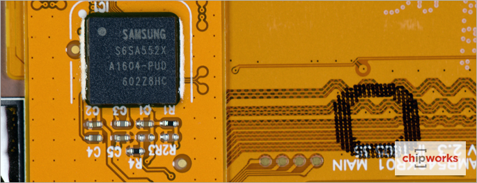
Touch Screen Controller
Touch Screen Controller
Our expectation that Samsung adopts their own touch screen controller (TSC) in their own phone was confirmed. The part number is S6SA552X. Chipworks first saw Samsung’s S6SMC41X TSC in a Chinese brand Doov L5Pro phone a few weeks ago. It is now our second time seeing Samsung’s TSC, but the first time in Samsung’s own phone.
RF Front End
As would be expected with a worldphone like the S7, there is plenty in its RF section. It is easiest to list them by manufacturer:
- Avago AFEM-9040 multiband multimode module
- EPCOS D5275 antenna switch module
- EPCOS D5287 antenna switch module
- Murata FAJ15 front end module
- Murata KM5D18098 Wi-Fi module
- Qorvo QM78064 high band RF fusion module
- Qorvo TQF6260 PA duplexer
- Qorvo QM63001A diversity receive module
- Qualcomm QFE3100 envelope tracker
- Qualcomm QFE2550 digital tuner
- Qualcomm WTR4905 transceiver
- Qualcomm WTR3925 transceiver
While not strictly in the RF front end, we have also found a NXP 67T05 NFC controller and an IDTP9221S for wireless charging.
What Else Do We Have?
We should also comment on the SK Hynix LPDDR4 SDRAM, which, according to SK Hynix’s databook, is the fastest LPDDR4 that they make at 3733 Mbps. As a commodity part, this uses a 366-ball package, so that does account for the density of solder bumps in the PoP – we count 342 in that.
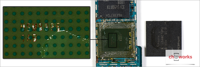
The flash is a Samsung KLUBG4G1CE 32 GB, universal flash storage (UFS), multi-level cell (MLC) part.
Other parts of note are:
- AKM AK09911 compass – we have seen this in over 60 phones!
- Bosch BMP280 pressure sensor
- DSP D4A1A audio/voice processor
- Knowles S1636 microphone
- Knowles S1638 microphone
- Maxim C551GY5A time-of-flight sensor
- Maxim MAX77854 PMIC
- Maxim MAX77838 PMIC
- Maxim MAX98506BEWV audio amplifier
- Qualcomm WCD9335 audio codec
- Qualcomm PM8996 PMIC
- Qualcomm PM8004 PMIC
- Samsung C3 image processor
- Samsung S2MPB02 PMIC – seen in multiple Samsung phones
- Samsung S6SA552X touch controller
- STMicroelectronics L2G2IS gyroscope