Posted: June 21, 2017
Contributing Authors: Ray Fontaine
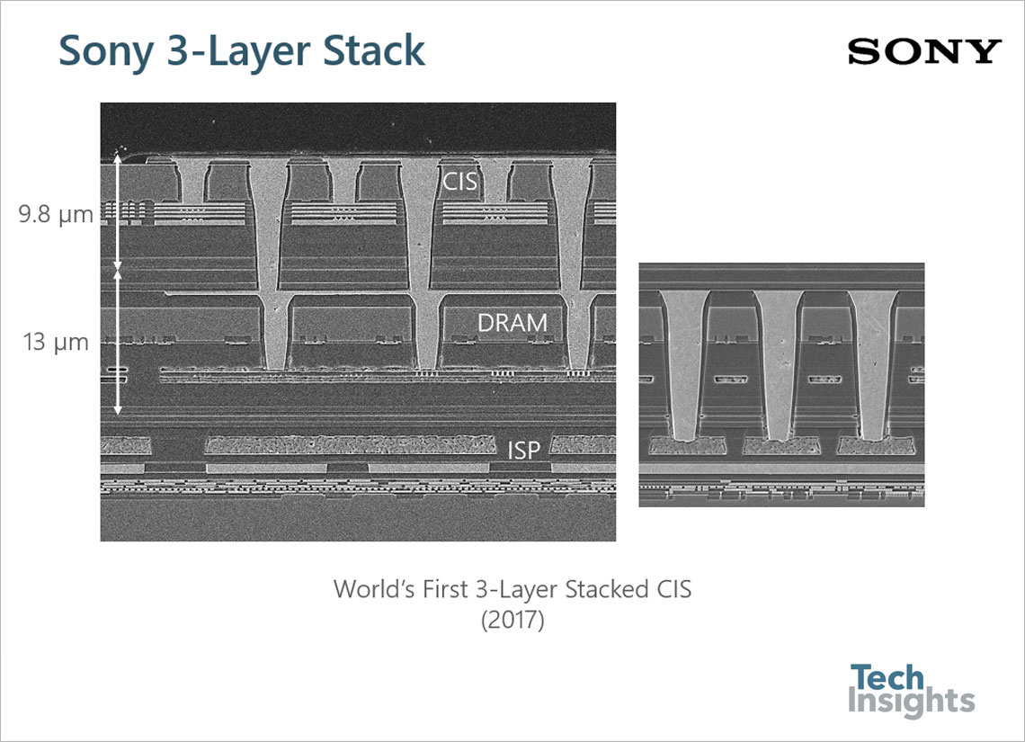
At the time of the IISW paper submission deadline in April, we hadn’t yet received the Sony Xperia XZs with 3-layer stacked Motion Eye camera. The technology development had been announced at ISSCC 2017, and we did get results in time for the presentation material (see also the blog by Dick James). Work on the IMX400 project continues and we look forward to publishing our report in a few weeks. Enjoy Part 2, where we discuss the trends in wafer-to-wafer interconnect and other features of stacked chips.

Stacked Chip Image Sensors
The development of low-temperature wafer bonding and various wafer-to-wafer interconnect techniques have been key enablers for stacked image sensors. Two-die stacks, comprising a back-illuminated CIS and mixed-signal image signal processor (ISP), have emerged as the dominant configuration for leading smartphone camera chips. The CIS portion can be considered a 'dumb' chip carrying only an active pixel array. Most of the signal chain and digital processing is partitioned onto the ISP and systems application processor.
| Chip Vendor | Year | Stacked CIS Foundry/Gen. | Stacked ISP Foundry/Gen. | |||
|---|---|---|---|---|---|---|
| Sony | 2013 | Sony 90 nm | Sony 65 nm | |||
| Sony | 2014 | Sony 90 nm | TSMC 40 nm | |||
| Sony | 2016 | Sony 90 nm | TSMC 28 nm | |||
| OmniVision | 2015 | XMC 65 nm | XMC 65 nm | |||
| OmniVision | 2016 | TSMC 65 nm | TSMC 65 nm | |||
| Samsung | 2015 | Samsung 65 nm | Samsung 65 nm | |||
| Samsung | 2016 | Samsung 65 nm | Samsung 28 nm HKMG | |||
| Sony | ISSCC 2017 |
|
||||
Table 2. Noteworthy Stacked Chip CIS/ISP Configurations
A. Stacked Chip Fabrication Technology Trend
The recent manufacturing trend for back-illuminated CIS chips in a stacked configuration seems to have stabilized at the 90/65 nm process generation. There doesn’t appear to be a driver for further scaling of the CIS chip technology generation, although recently sub-65 nm processing has been observed in 1.0 µm generation pixel structures to facilitate narrower W aperture grid metal. Samsung’s 28 nm high-k metal gate process is currently in use for stacked ISPs [14] and the ISP scaling trend is expected to continue towards the latest advanced CMOS technology generations.

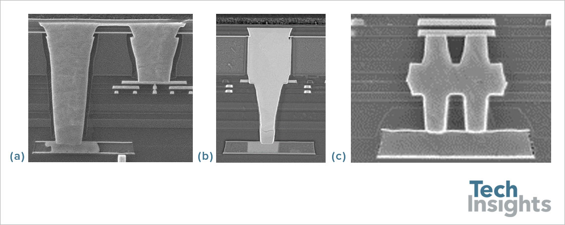
Fig. 1. Sony 1st gen. dual TSVs (a), 2nd gen. unified TSV (b), 1st gen. DBI (c)

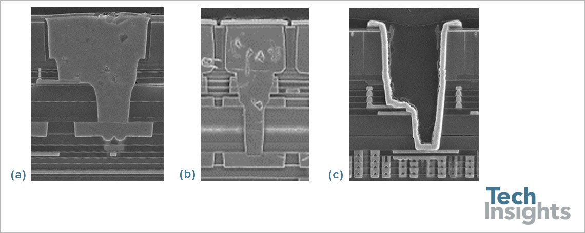
Fig. 2. OmniVision 1st gen. butted TSV (a), 2nd gen. unified TSV (b), Samsung butted TSV (c)
B. Wafer-to-Wafer Interconnect
Sony was first to bring stacked CIS chips to market, initially by implementing homogenous wafer-to-wafer bonding (oxide bonding) and through-silicon-vias (TSVs) in 2013 and later with Cu-to-Cu hybrid bonding, also known as Cu2Cu bonding or DBI, in 2016 [18,19]. The first generation TSVs, deployed as three major arrays above and along both sides of the active pixel array, featured a dual TSV structure for the row/column interconnect of a 1.12 µm generation pixel array. One shallow, Cu-filled TSV contacted the back of a metal 1 CIS metal pad, one deep, Cu-filled TSV contacted a top metal Al ISP pad, and final interconnect was achieved with a planar Cu metal strap. The dual TSV structures had a rectangular footprint and were placed on a 6.0 µm x 9.0 µm orthogonal pitch [20].
TSony simplified its TSV process flow in 2015 by introducing a single, or ‘unified’, structure which contacted both CIS and ISP landing pads with one cylindrical vertical interconnect [21]. These structures were placed on a 9.1 µm minimum orthogonal pitch, although TSV rows were half-pitch staggered from neighboring rows.
OmniVision’s first observed stacked chips, fabricated on the PureCel-S platform with foundry partner XMC, featured a ‘butted’ TSV structure in which a single, wide TSV contacted both a CIS and ISP pad structure. The rectangular structures, in use on a 1.12 µm pixel generation chip, had a 5.2 µm x 9.9 µm orthogonal pitch [22]. OmniVision later adopted a unified TSV structure for its 1.0 µm pixel generation PureCelPlus-S chips, fabricated by foundry partner TSMC. These structures were placed on a 4.0 µm x 4.1 µm orthogonal pitch [10].
The observed Samsung stacked chips in production also feature a butted TSV structure, but instead use a W-based TSV window liner for vertical interconnect. The first-generation Samsung TSVs, incorporated on a 1.12 µm pixel generation chip, were placed on an 8.8 µm x 9.6 µm orthogonal pitch [23].
Sony recently shifted its interconnect strategy to incorporate DBI initially as a TSV array replacement. This implementation of DBI featured active DBI pads in the same regions as had been occupied by TSVs, with dummy DBI pads covering most of the active pixel array and peripheral regions. The current state of the art for production DBI is square pads having a 3.0 µm width placed on a 6.0 µm orthogonal pitch. A DBI pitch of 1.6 µm has been reported [24] and it is expected that future generations of DBI-enabled chips will feature per-pixel interconnect.

Get regular, succinct analysis of high-volume imaging and emerging applications
References
[1] FujiFilm press release, Jul. 21, 2010.
[2] “Fujifilm MS3961 Die Markings 12.0 MP, 1.6 μm Pixel Size CCD Image Sensor from Fujifilm FinePix Z800EXR Focused Technology Analysis (FTA) Report”, IPR-1009-801-01, -03, -04, -05, Oct. 2010.
[3] Nikon press release, Sep. 2011.
[4] “Aptina MT9J007C1HS 12 Megapixel (10.1 Megapixel Effective) CMOS Image Sensor with DR-Pix™ Technology from a Nikon V1 Camera Imager Process Review”, IPR-1110-804, Dec. 2011. [5] Canon EOS 650D press release, Jun. 2012.
[6] “Canon LC1270 18.0 MP, 4.3 μm Pixel Size, APS-C Format CMOS Image Sensor from Canon EOS Rebel T4i (EOS 650D/EOS Kiss X6i)”, IPR-1206-802, Aug. 2012.
[7] “Sony IMX270, Micro Four Thirds, 20.4 MP Resolution, 3.3 µm Pixel Pitch, Front-Illuminated “Live MOS” CMOS Image Sensor from Olympus OM-D E-M1 Mark II MILC”, DEF-1703-802, Apr. 2017.
[8] Fujifilm press release, Jan. 2013.
[9] “Toshiba TCM5112CL CMOS Image Sensor from Fujifilm X20 Device Essentials Summary”, DEF-1311-803, Nov. 2013.
[10] “OmniVision OV16880, 1/3.06” Format, 16 MP Resolution, 1.0 μm Pixel Pitch Stacked (PureCel Plus-S) Back-Illuminated CMOS Image Sensor”, DEF-1606-804, Aug. 2016.
[11] Sony Xperia Z5 product page, Oct. 2015.
[12] Canon EOS 70D press release, Jul. 2013.
[13] Samsung press release, Mar. 2016.
[14] “Samsung S5K2L1, 1/2.6” Format, 12 MP Resolution, 1.4 μm Pixel Pitch Back-Illuminated Stacked ISOCELL CMOS Image Sensor from Samsung Galaxy S7 (Model SM-G930FD)”, DEF-1603-804, Apr. 2016.
[15] “Sony IMX260 12 MP, 1.4 μm Pixel Pitch Stacked BI CIS with DBI and Full Chip PDAF from the Samsung Galaxy S7 edge Rear-Facing Camera Imager Process Review”, IPR-1603-802, May 16, 2016.
[16] “Sony 12 MP Resolution, 1.0 μm Pixel Generation Stacked (Exmor RS) Back-Illuminated CMOS Image Sensor from iPhone 7 Plus Telephoto iSight Camera”, DEF-1612-801, Jan. 2017.
[17] Oppo R9s landing page, Oct. 2016.
[18] Kagawa, et. al, “Novel Stacked CMOS Image Sensor with Advanced Cu2C2 Hybrid Bonding” ISSCC2017. Feb. 2017.
[19] Invensas corporate web site, Apr. 2017.
[20] “Sony ISX014 1/4 Inch 8 MP, 1.12 μm Pixel Size Exmor RS Stacked Back Illuminated CIS Imager Process Review”, IPR-1302-801, Mar. 2013.
[21] “Sony IMX278 13.0 MP Exmor RS™ RGBW Stacked BI CMOS Image Sensor Extracted from the Huawei P8 Imager Process Review”, IPR-1505-801, Jul. 2015.
[22] “OmniVision OV23850 PureCel-S 1.12 μm Pixel, 23.8 MP Stacked CMOS Image Sensor from Gionee GN9008”, DEF-1508-802, Sep. 2015.
[23] “Samsung S5K3M2 13 MP Stacked, ISOCELL CMOS Image Sensor from Vivo X5Pro”, DEF-1507-801, Jul. 2015.
[24] P. Enquist, “Stacked image sensors - the new image sensor standard”, 2015 Image Sensors Europe, Mar. 2015.
[25] “STMicroelectronics 5 MP, 1.4 μm Pixel Pitch CMOS Image Sensor (5953BA Die Markings) Imager Process Review”, IPR-1003-802, Apr. 2010.
[26] “Sony IMX147 20 MP, 1.2 μm Pixel Pitch Back Illuminated (Exmor R) CMOS Image Sensor from the Sony Cyber-shot HX300 Digital Compact Camera”, IPR-1307-801, Sep. 2013.
[27] “Samsung S5K3P3SX 16 MP, 1.0 μm Pixel Pitch Stacked BSI Full ISOCELL CIS from the Samsung Galaxy A8 Smartphone Primary Camera Imager Process Review”, IPR-1509-801, Jan. 2016.


