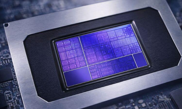
This report contains the following detailed information:
- Selected teardown photographs, package photographs, package X-rays, die markings, and die photographs
- Scanning electron microscopy (SEM) cross-sectional micrographs of the general structure of the redundancy memory
- Measurements of vertical and horizontal dimensions of the redundancy memory
- Plan-view optical micrographs of the die delayered to the polysilicon layer


