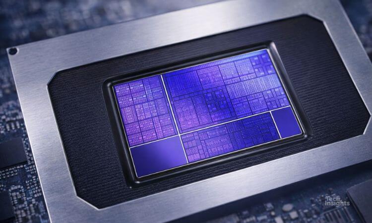
This report contains the following detailed information:
- Selected teardown photographs, package photographs, package X-rays, die markings, and die photographs
- SEM cross-sectional micrographs of the general structure of the die dielectric materials, major features, and transistors
- Plan-view SEM micrograph of the memory array delayered to active, WL, and BL layers
- Measurements of vertical and horizontal dimensions of major microstructural features
- Plan-view optical micrograph of the die delayered to the polysilicon layer
- Identification of major functional blocks on a polysilicon die photograph
- Table of functional block sizes and percentage die utilization
- High-resolution top metal and diffusion level die photographs delivered in the CircuitVision software


