A History of Chiplets: Revolutionizing Chip Design
The history of chiplet technology is intricately linked to the ever-evolving nature of the semiconductor industry. Let's delve into the key milestones that shaped the rise of chiplets and their impact on design approaches.
Makimoto's Wave and the Cycle of Integration
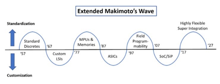
In 1991, Dr. Tsugio Makimoto observed a fascinating pattern in the industry: a cyclical shift between standardization and customization roughly every decade. This concept, known as Makimoto's Wave, accurately predicted the industry's progression from standard discrete components in the 1950s to the rise of Application-Specific Integrated Circuits (ASICs) in the late 1980s and early 1990s. The following decade saw the dominance of Field-Programmable Gate Arrays (FPGAs), followed by the era of System-on-Chip (SoC) and System-in-Package (SiP) solutions.
Extended Makimoto's Wave. Source: Makimoto, Tsugio. "Implications of Makimoto's Wave," IEEE Computer, Vol. 46, pp. 32-37, 2013.
The current decade (2017-2027) marks the fourth swing towards standardization in Makimoto's Wave, characterized by the emergence of chiplet-based design and enabled by advancements in leading-edge packaging technologies.
Moore's Law and the Seeds of Disaggregation
Even earlier, in his seminal 1965 paper "Cramming More Components Onto Integrated Circuits," Gordon Moore foresaw the limitations of monolithic SoCs. Besides being the author of Moore’s Law, Moore famously stated, "It may prove to be more economical to build large systems out of smaller functions, which are separately packaged and interconnected." This statement laid the groundwork for the concept of heterogeneous integration, a cornerstone of chiplet technology.
From Multi-Chip Modules to Advanced Packaging
Traditional packaging served the primary purpose of protecting chips and enabling connections to other devices. Multi-chip Modules (MCMs) offered a glimpse into the future of modularity, but limitations in technology and high costs hindered their widespread adoption.
Advanced packaging emerged to address these limitations, offering significant performance improvements compared to traditional methods and enabling miniaturization. Key advancements include wafer-level packaging in the 2000s, followed by 2.5D and 3D stacking technologies that leveraged through-silicon vias (TSVs).
The Rise of Chiplets and a New Design Paradigm
Chiplet technology, fueled by advancements in packaging, has become a disruptive force in the industry, fundamentally altering how chips are designed. The core concept is the disaggregation of a large SoC design into smaller, functionally specialized chiplets. Imagine building with blocks – each chiplet performs a specific task, such as housing CPU cores or a memory controller.
These "known good die" are then interconnected within a package, offering several key advantages:
- Mix-and-Match Flexibility: Chiplets can be sourced from different vendors and manufactured using the most suitable process node for each function. This enables unmatched flexibility and performance optimization.
- Faster Time to Market and Reduced Costs: By leveraging pre-designed chiplets, design teams can focus on integration and customization within their SoCs, leading to faster development cycles and lower overall costs.
- Improved Yields: Defective chiplets can be replaced without scrapping the entire SoC, boosting yield and cost-effectiveness.
Chiplets vs. Monolithic SoCs: Weighing the Options
While chiplets offer a compelling design approach, it's important to understand the trade-offs with traditional monolithic SoCs:
Chiplet Advantages:
- Mix-and-Match Flexibility
- Faster Time to Market and Lower Costs
- Improved Yields
Chiplet Disadvantages:
- Complex Interconnect Design
- Thermal Management Challenges (especially in stacked configurations)
Monolithic SoC Advantages:
- Tight Integration & Superior Performance
- Lower Latency
Monolithic SoC Disadvantages:
- Longer Development Cycles
- Lower Yields & Higher Cost
The Future of Chiplet Technology
The future of chip design is inextricably linked to chiplets. As the technology matures, the chiplet ecosystem will continue to develop, offering a wider range of pre-designed, high-quality chiplets.
For the full story on chiplets, the history, applications, and forecasts, read Chiplet Market Introduction: Computing.
TechInsights’ 2026 Outlook Summit Series
TechInsights’ 2026 Outlook Summit brings together leading semiconductor experts to decode the year ahead.
Supreme Court Strikes Down IEEPA Tariffs | Semiconductor Impact
The Supreme Court invalidates IEEPA tariffs as the U.S.-Taiwan trade deal reshapes semiconductor import policy. Read the TechInsights report.
Chip Observer: CES 2026, AI Power Plays, and a $48B M&A Surge
CES 2026 semiconductor news: AI PCs, Snapdragon X2 Elite, $48B in M&A, ZAM memory, and a 2026 forecast projecting a $1 trillion chip market.
Intel Panther Lake on Intel 18A: Strategic & Geopolitical Analysis
Explore Intel Panther Lake on Intel 18A, examining advanced-node execution, IDM 2.0 credibility, and strategic implications for the global semiconductor ecosystem.


