Apple iPhone 8 Plus Teardown
Posted: September 10, 2017, Updated: October 11, 2017
Contributing Authors: Daniel Yang, Stacy Wegner, Ray Fontaine
A11 Bionic Application Processor
Applications Processor
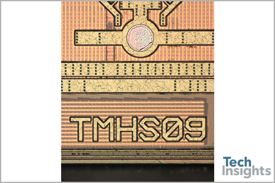
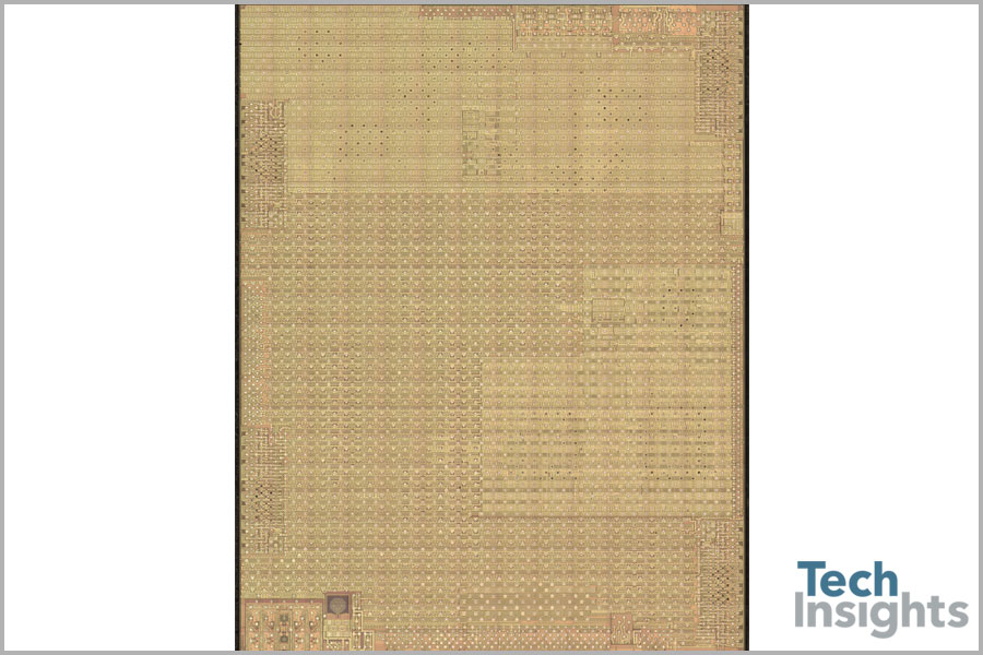
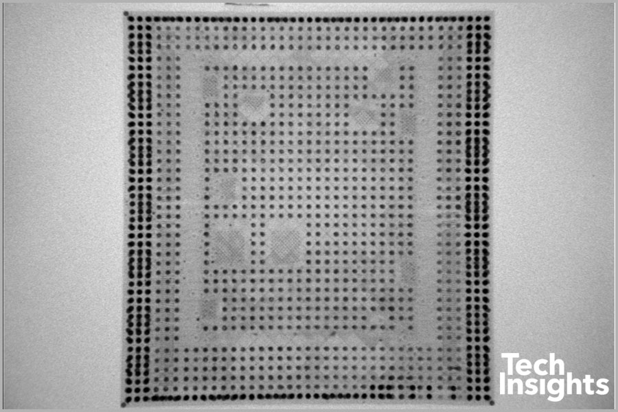
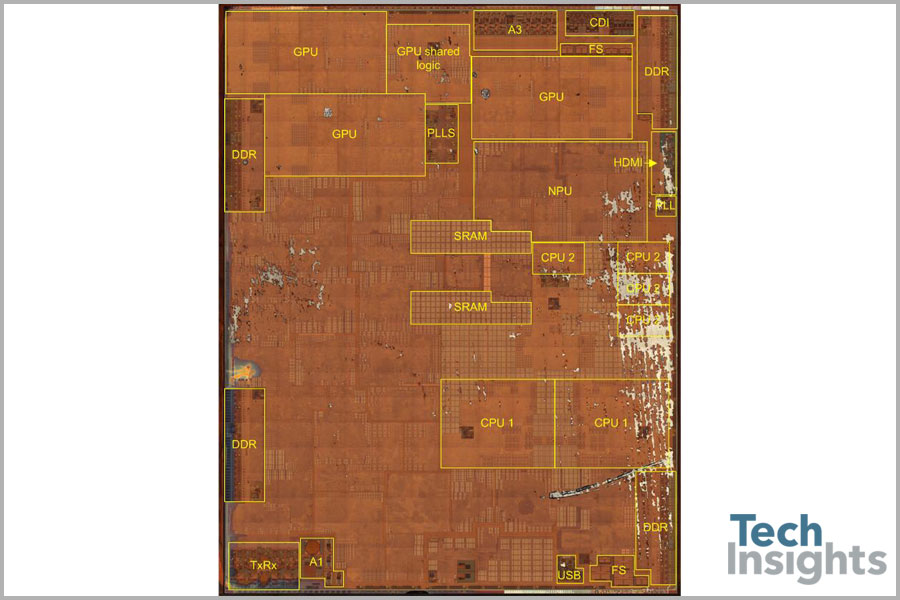
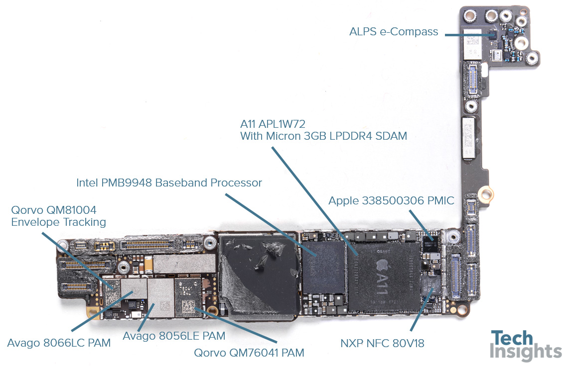
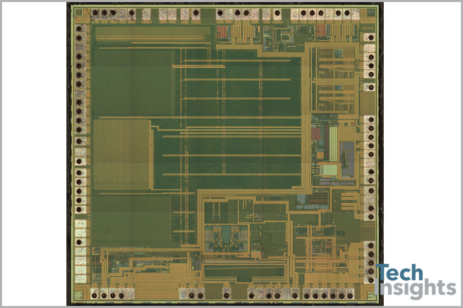
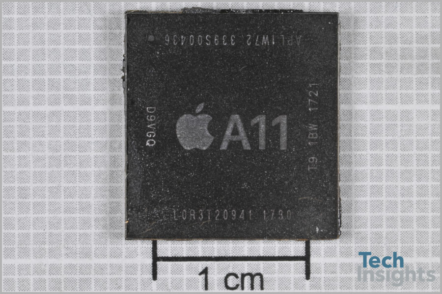
The iPhone 8 Plus A1897 model we examined initially is confirmed to contain the A11 Bionic AP with a die mark TMHS09. The A11 is a Package on Package (PoP) with the Micron MT53D384M64D4NY 3GB Mobile LPDDR4x SDRAM. The die size (seal) is 87.66 mm2, representing a 30% die shrink compared to the A10. The biggest new feature of the AP at announcement is a dedicated “Neural Engine” primarily for Face ID on the iPhone X, but being an inference engine, it could also be used to improve Siri as well as for AR applications. This should be an Apple custom design based on Apple’s multiple AI startup company acquisitions in recent years. While this inference-based core may not be fully utilized in the iPhone 8, we will not have to wait for the iPhone X to start analyzing and delayering it, for a deeper look at the IP.
A11 Details:
- 30% die area shrink compared to A10
- Big blocks keep this trend: CPU1 is smaller by 30%, GPU is smaller by 40% and SDRAM interface is smaller by 40%
- There is more CPU2 on the A11 than on the A10 (they now use 4 little cores, and before they used only 2). First time we noticed was on the A10
- In relative numbers they are pretty similar: CPUs take about 15%, GPU takes about 20%, SDRAM interface takes about 8%
- GPU remains the same 6-core GPU with common logic
- General location of the blocks is strikingly similar to the A10
So far the biggest difference from the A10 is the addition of the NPU. But is it really the NPU? If you are interested in getting the answer, please contact TechInsights for the upcoming Apple A11 Bionic Application Processor Digital Functional Analysis Report (FAR-1709-802).
Download a complimentary sample report from our mobile devices teardown subscription
iPhone 8/8 Plus Cameras
Phil Schiller introduced us to iPhone 8's cameras beginning with the A11 Bionic's specs, which include a new Apple-designed image signal processor (ISP) that helps improve autofocus (AF) performance in low-light, and features pixel processing for enhanced sharpness and texture. rst time, the ISP on iPhone’s application processor (AP) features hardware-enabled multi-band noise reduction. Of course, this new AP functionality complements the processing done on the stacked chip image sensors’ companion ISPs.
As for the image sensors, Mr. Schiller commented at launch that while there is no change for the iPhone 8 camera resolution, the rear-facing 12 MP camera features a new, larger CIS. iPhone 8 Plus uses a dual camera system adding a telephoto camera with 12 MP CIS. The FaceTime camera resolution remains unchanged at 7 MP. We don’t recall hearing the term ‘iSight’ during the September 22 event, and it appears the iSight sub-branding has been dropped from Apple’s iPhone product specification pages. Regardless, the new CIS is reported to feature “deeper pixels”, and a new color filter. Mr. Schiller also mentioned the 12 MP cameras are more power efficient. Our initial speculation on this statement is iPhone 8's stacked chip camera ISPs might now be fabricated using TSMC's 28 nm line. Since Apple started using Sony stacked (Exmor RS) image sensors in 2013 (iPhone 5s) we have found iPhone’s camera ISPs fabricated with either 65 nm or 40 nm generation process technology. Sony has previously used TSMC 28 nm generation ISPs for its own IMX318, but we haven’t seen that in an Apple product yet. There is also the possibility the camera chip’s ISP is fabricated using FD-SOI. Recalling Junko Yoshida of EETimes’ 2016 article[1], Sony was rumored to be exploring FD-SOI for stacked imager ISPs.
The video performance is claimed to be the highest quality video capture available in a smartphone. The A11 also features an Apple-designed video encoder enabling 4K video at 60 fps and Slo-mo 1080p video at 240 fps. Augmented reality (AR) was prominently featured in the September 22nd announcement, and the iPhone 8 is claimed to be the first smartphone with substantial customization for AR. As mentioned in February [2], Tim Cook and Team Apple consider AR to be the next big thing and the camera modules are apparently individually calibrated with AR in mind.
We’ll be providing deeper technical analysis through our Image Sensor subscription service as well as through the following TechInsights Open Market Reports:
- DEF-1709-802: Apple iPhone 8 Plus Wide-Angle Camera 12 MP Image Sensor Device Essentials Image Set and Summary
- DEF-1709-803: Apple iPhone 8 Plus Telephoto Camera 12 MP Image Sensor Device Essentials Image Set and Summary
- DEF-1709-804: Apple iPhone 8 Plus FaceTime Camera 7 MP Image Sensor Device Essentials Image Set and Summary
In the meantime, we’re happy to share the following preliminary camera-related findings below:
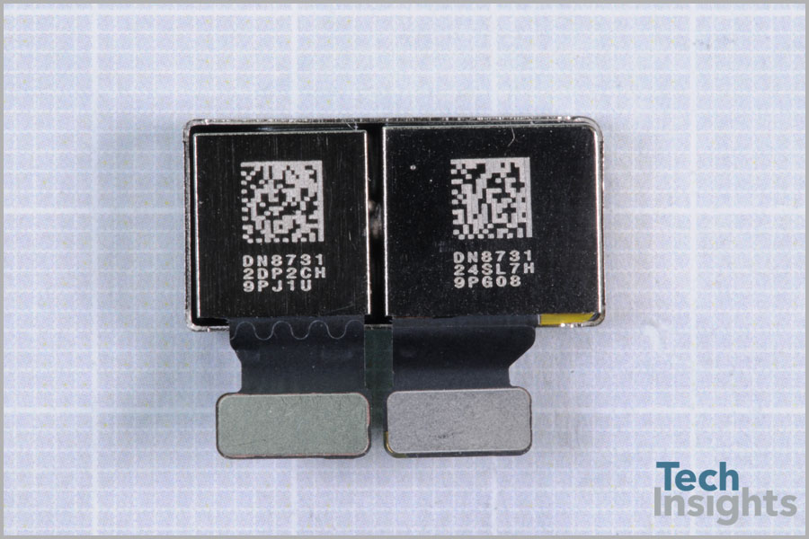
Dual Rear-Facing Cameras
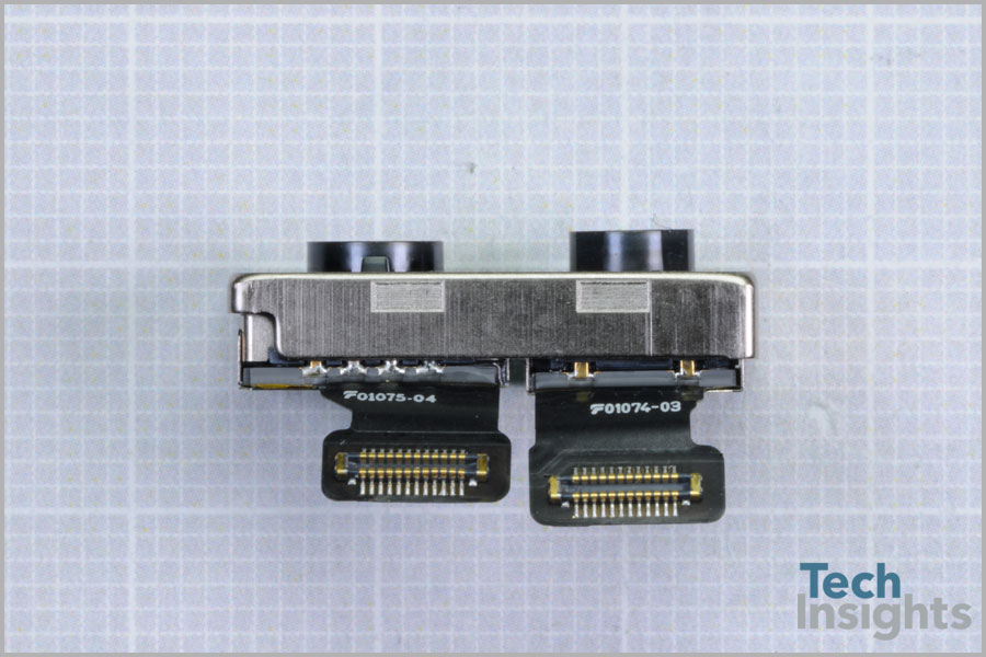
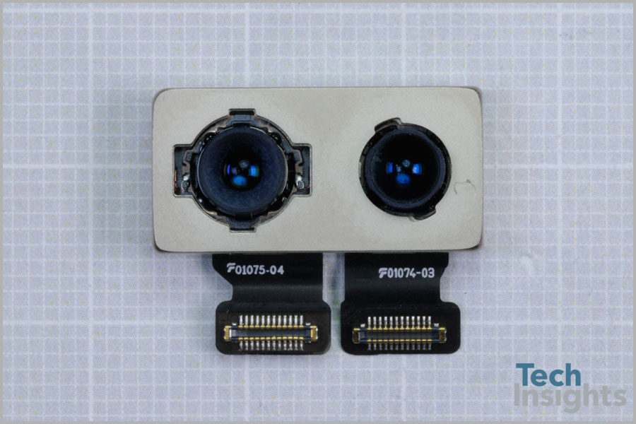
Dual Rear-Facing Cameras (12 MP Wide-Angle and 12 MP Telephoto)
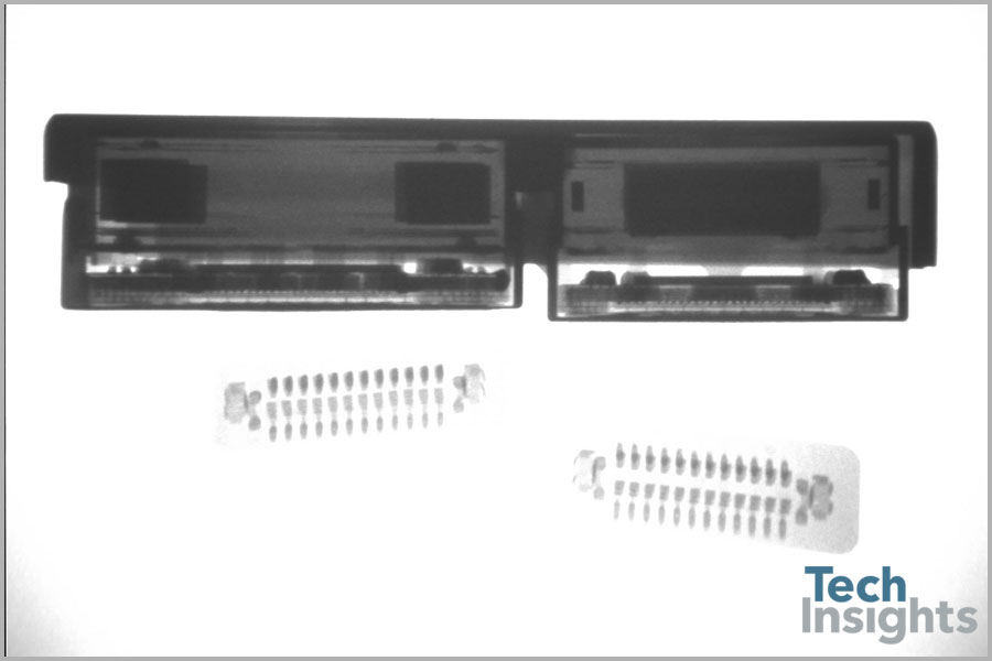
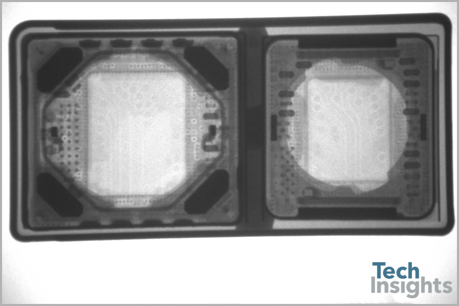
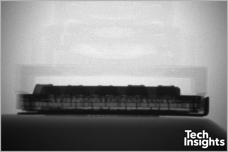
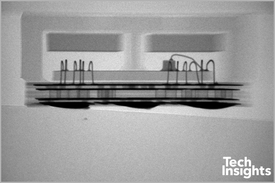
The dual camera module size is 21.0 mm x 10.6 mm x 6.3 mm thick. Based on our initial X-rays it appears the wide-angle camera uses optical image stabilization (OIS), while the telephoto camera does not (the same configuration as iPhone 7 Plus).
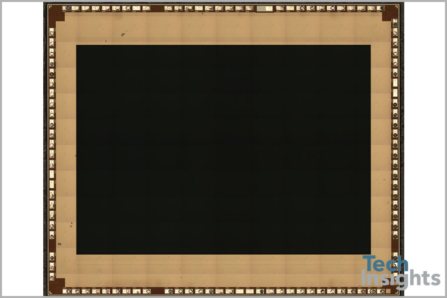
Dual Rear-Facing Camera Die
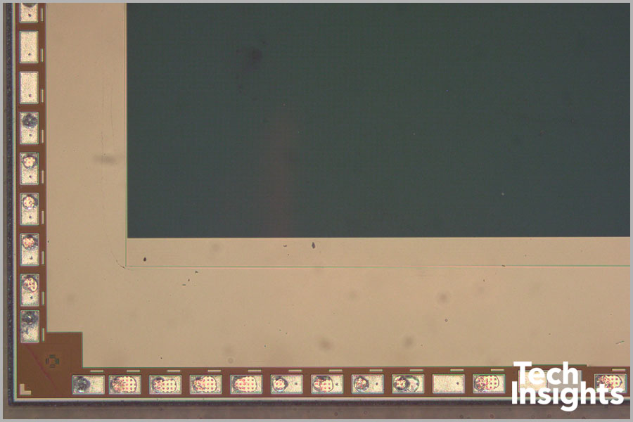
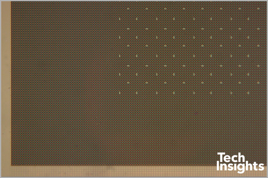
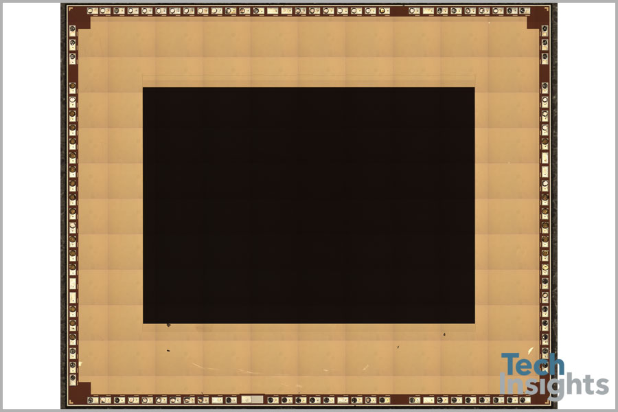
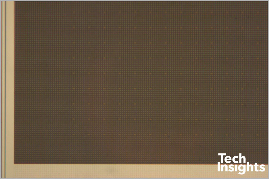
The wide-angle Sony CIS has a die size of 6.29 mm x 5.21 mm (32.8 mm2). This compares to a 32.3 mm2 die size for iPhone 7’s wide-angle CIS. We can confirm a 1.22 µm pixel pitch. We note a new Phase Pixel pattern, but the big news is the absence of surface artifacts corresponding through to the silicon via (TSV) arrays we have seen for a few years. A superficial review of the die photo would suggest it is a regular back-illuminated (BSI) chip. However, we have confirmed it is a stacked (Exmor RS) chip which means hybrid bonding is in use for the first time in an Apple camera!

7 MP Front-Facing Camera
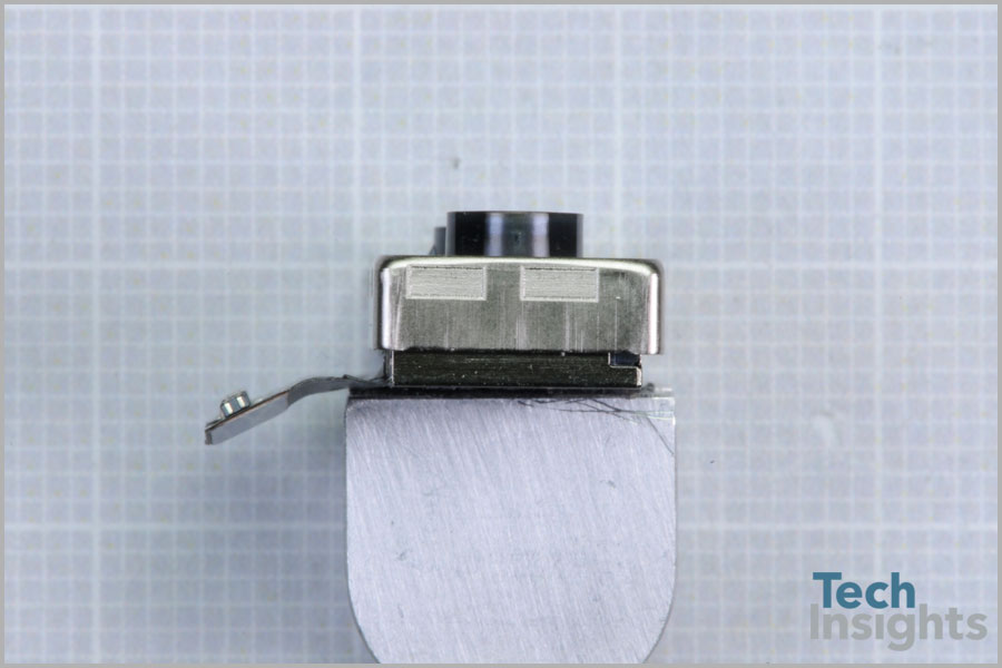
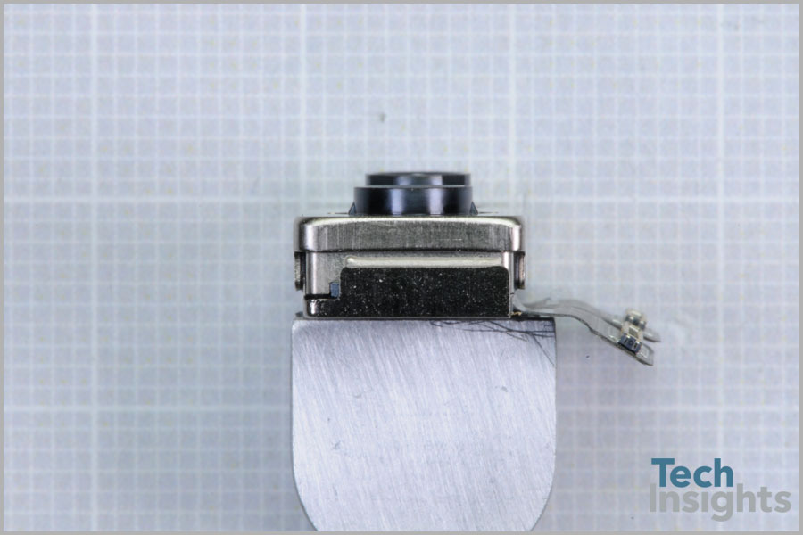
7 MP Front-Facing Camera
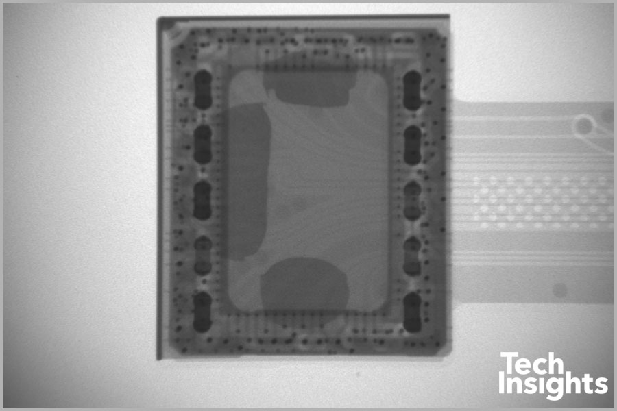
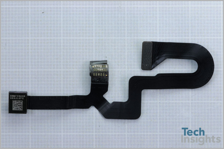
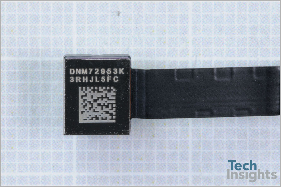
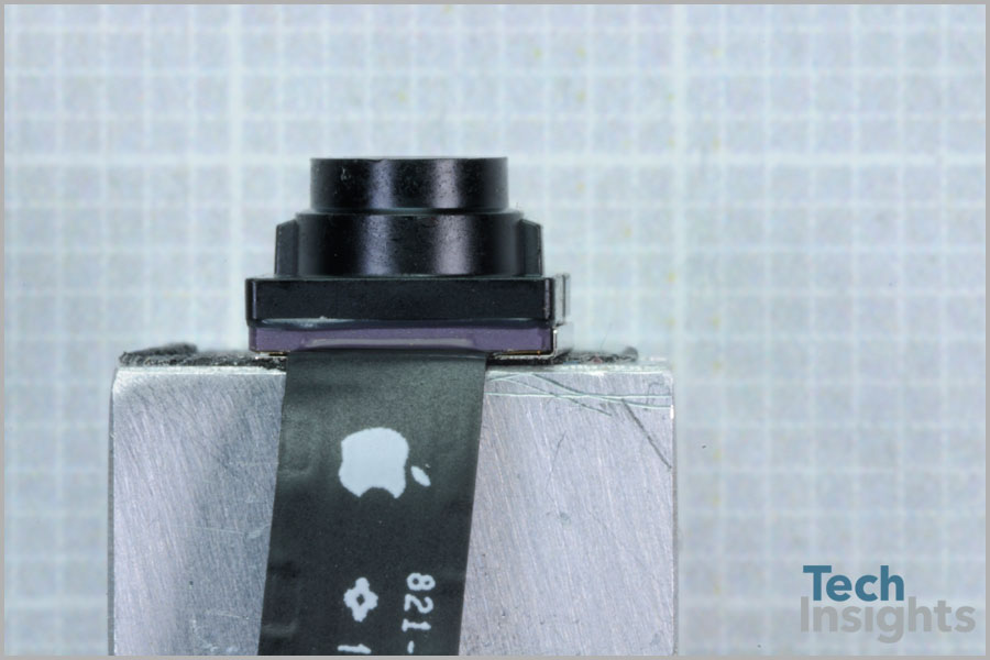
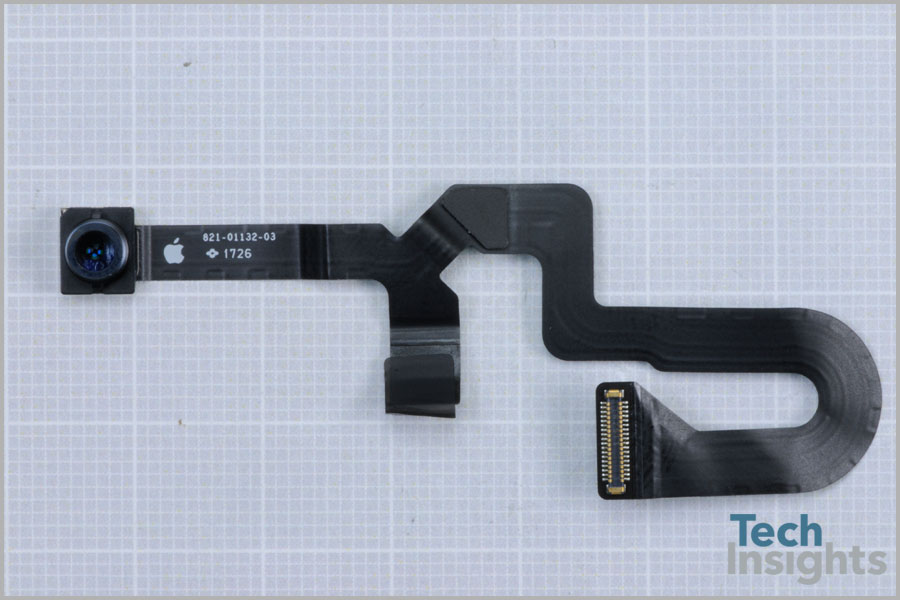
The front-facing camera module size is 6.8 X mm x 5.8 mm x 4.4 mm thick.
The front-facing Sony CIS die size is 3.73 mm x 5.05 mm (18.8 mm2) and has a pixel pitch of 1.0 µm. Both are metrics are aligned with iPhone 7’s front-facing camera, however we also noted the absence of TSVs so we’ll be doing more work to explore the hybrid bonding on this Exmor RS die.
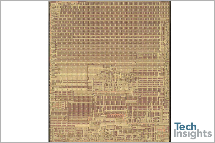
Intel XMM7480 Modem
Baseband
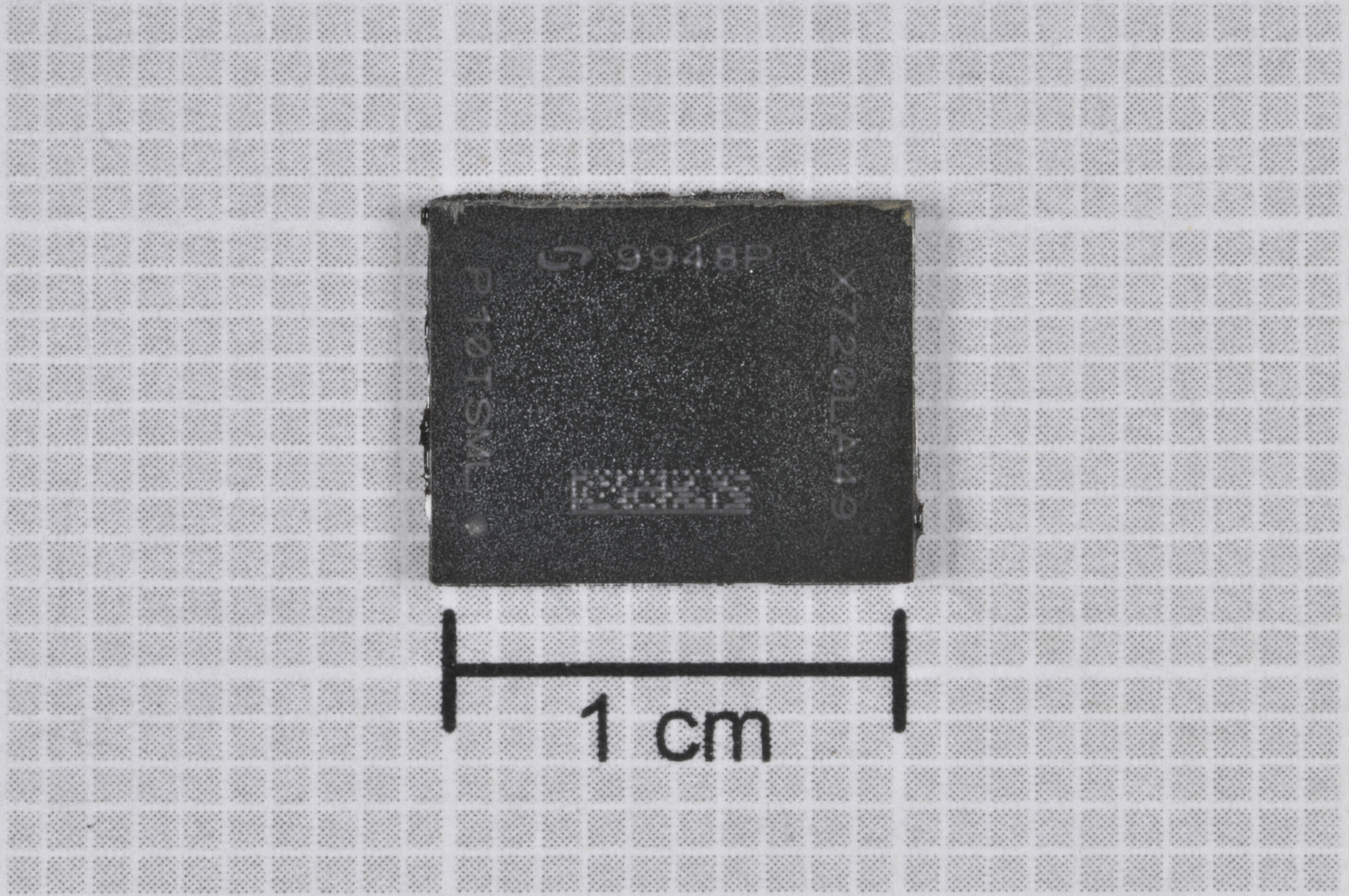
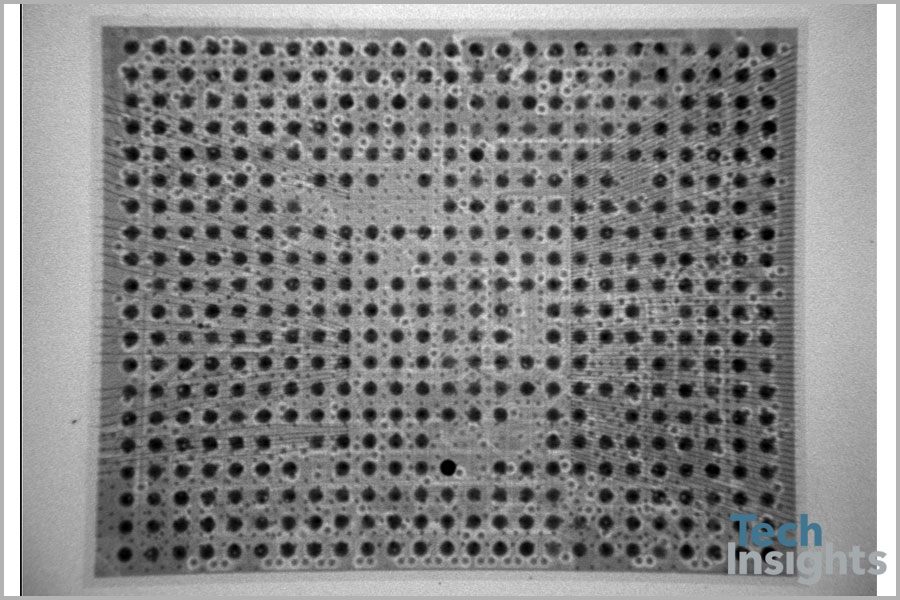
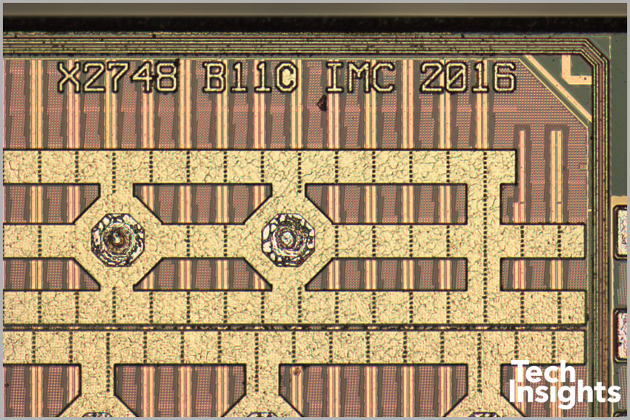
The iPhone 8 Plus A1897 model we examined initially is an Intel solution based phone. We see Intel’s next generation Baseband Processor (Modem) the PMB9948. We found the die marks to be “X2748 B11”. It is Intel’s XMM7480 modem and is the company’s fourth-generation LTE modem.
The XMM7480 (PMB9948) modem die size is 7.70mm x 9.15mm (70.45mm2), bigger than the previous generation XMM7360 (PMB9943) which is 7.71mm x 8.47mm (65.30mm2). Please contact TechInsights for the upcoming Intel XMM7480 (PMB9948) Modem Digital Functional Analysis Report (FAR-1709-803).
Intel PMB5757 RF Transceiver
RF Transceiver
The Transceiver is new Intel Trx, the PMB5757. After comparing the die photos of the Intel PMB5757 RF Transceiver to the previous PMB5750 used in the iPhone 7/7 Plus, it appears that Intel has re-used most of the previous chip. The two dies are in the same die size and they are almost identical except for minor changes in the left column and bottom row of repeated cells.
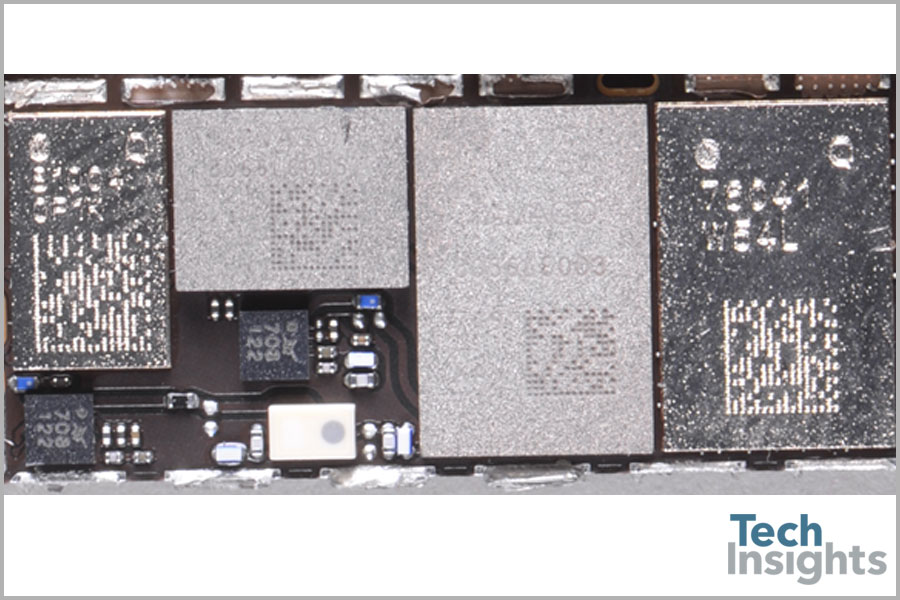
The balance of the RF front end looks much like the iPhone 7 with the following observations on winners in our iPhone 8 Plus; Envelope tracking goes to Qorvo 81004, High-band PAMiD goes to Broadcom 8066LC005, Mid-band PAMiD goes to Broadcom 8056LE003 and the Low-band PAMiD goes to Qorvo 76041.
Power Management ICs
Intel PMB6848 (also known as the X-PMU 748). Apple/Dialog Semiconductor 338S00309, and 338S00306. Compared to the iPhone 7, there is one more PMIC component from Dialog in the iPhone 8 Plus.
Flash Memory
The version of the phone we examined first is equipped with a SK Hynix H23Q2T8QK6MES-BC 256GB NAND Flash. We have confirmed that it is SK Hynix’s 48-Layer 3D NAND Flash. More information will be available in the upcoming SK Hynix 48L 3D NAND aCMOS Essentials report (ACE-1710-801).
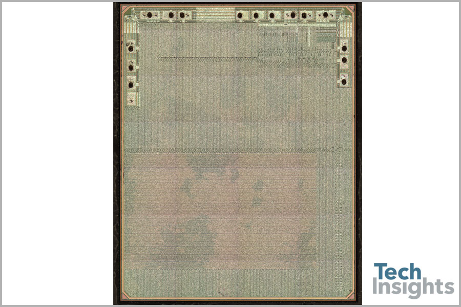
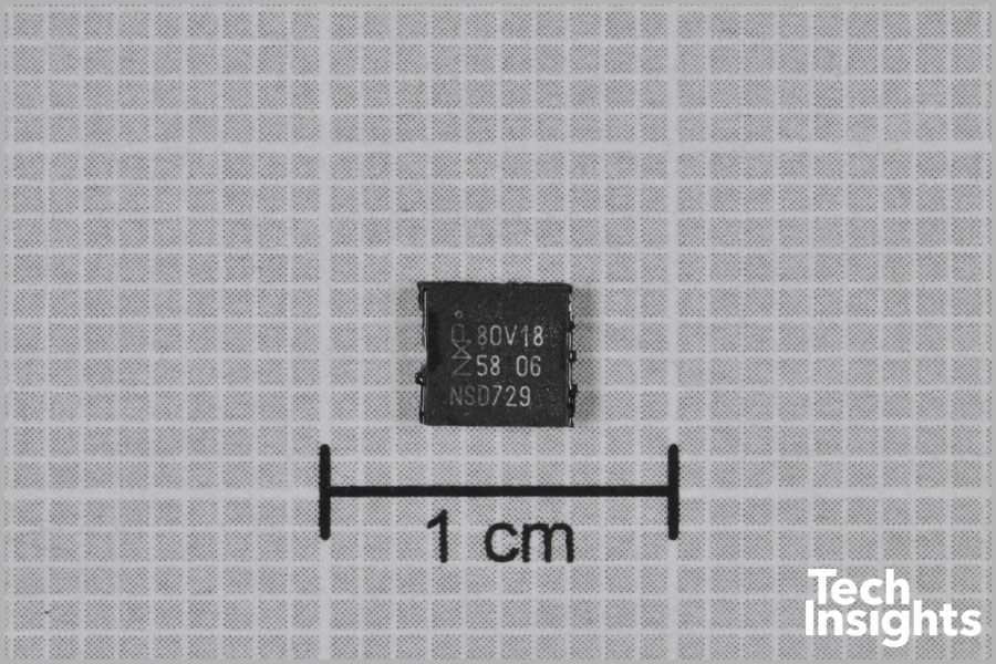
NXP PN64V iPhone 7 Plus A1784
NFC Controller
We were not too surprised to find a NXP NFC module in the iPhone 8 Plus. This one has package markings ‘80V18’. This is different from the PN67V we found in the iPhone 7 Plus.
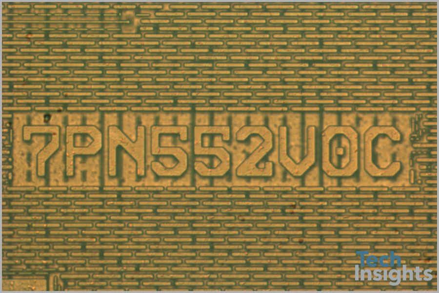
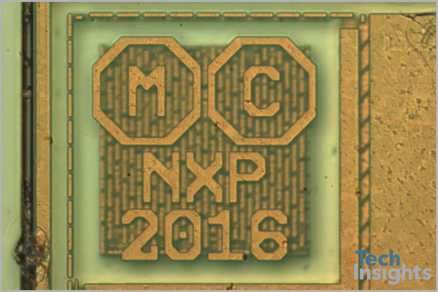
Again, our lab has got the die marks 7PN552V0C of the controller die.
From the floorplan view, the NFC Controller die in the iPhone 8 Plus is almost the same as the PN80T NFC Controller die in the Samsung Galaxy S8/S8 Plus series phones. The iPhone 8 Plus NFC Controller Security Element die is also very similar to the die in the Samsung Galaxy S8/S8 Plus series phones. TechInsights has previously analyzed the Samsung Galaxy S8 PN80T NFC Controller die and Security Element die. The PN80T NFC Controller die is fabbed in 180 nm node and the Security Element die is fabbed in 40 nm eFlash.
Wi-Fi/BT Module
Wi-Fi/BT Module
The iPhone 8 Plus we examined contains the Universal Scientific Industrial (USI) 339S00397 Wi-Fi/Bluetooth module. Apple announced that the iPhone 8 and 8 Plus support Bluetooth 5.0, so we initially suspected that the wireless combo chip in the USI module might be the Broadcom BCM4361, and our analysis has confirmed that we are correct. Broadcom wins the wireless combo socket. TechInsights previously analyzed the Broadcom BCM4361 wireless combo SoC when we found it in our Samsung Galaxy S8 analyses.
Other than the BCM4361, TechInsights has also analyzed other Bluetooth 5.0 SoCs, including Texas Instruments CC2640R2F, Qualcomm WCN3990, and a dialog DA14586. We also have die photos ready of the Nordic nRF52840 Bluetooth 5.0 soC.
The USI 339S00397 module has a total of 15 dies. Broadcom BCM4357 is the 5G Wi-Fi 802.11ac and Bluetooth 5.0 wireless combo IC. According to Broadcom, it also supports FM radio. We have depotted the BCM4357 and see the die marks: BCM43572. We think that the “2” may represent a revision number. Why? In the Samsung Galaxy S8 teardown, we found the Broadcom BCM4361 5G Wi-Fi 802.11ac and the Bluetooth 5.0 wireless combo IC in the Murata module KM7206044. The BCM4361 was the industry’s first Bluetooth 5.0 supported SoC at that time.
If we compare the die marks and die photos of the Broadcom BCM4357 from the iPhone 8 Plus and the BCM4361 from the Galaxy S8, they are the same die. We cannot see any major differences in the die floorplan. TechInsights has completed Digital Functional Analysis on the Broadcom BCM4361 (die BCM43570).
Audio ICs
We see three 338S00295 Audio Amplifiers. They should be from Apple/Cirrus Logic. The 338S00248 is the Audio Codec from Apple/Cirrus Logic too.
USB Interface
A Cypress EZ-PD™ CCG2 USB Type-C Port Controller is found in the iPhone 8 Plus. We decoded the part number as CYPD2104. The chip enables fast charging for the iPhone when coupled with a compatible accessory Apple USB-C power adapter (29W Model A1540). We have already seen it in the iPad Pro 10.5 ‘’ in June 2017.
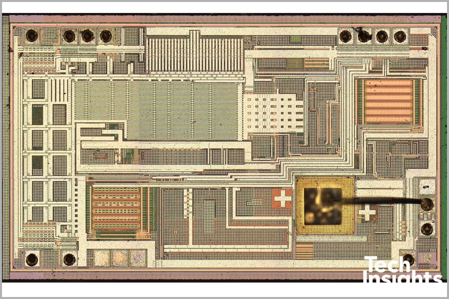
Time-of-Flight (ToF)
Time-of-Flight (ToF)
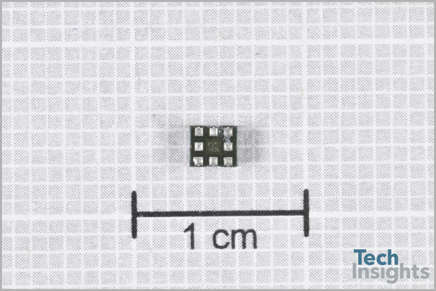
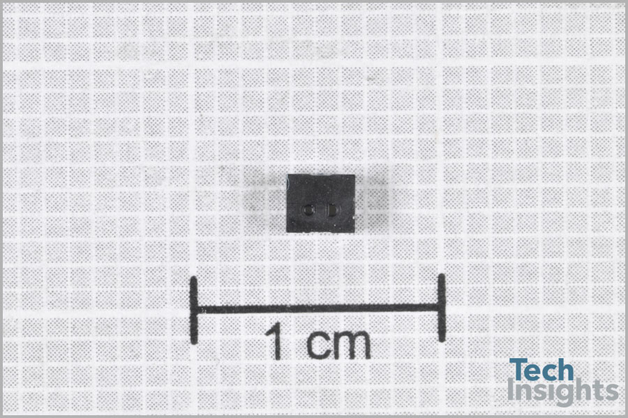
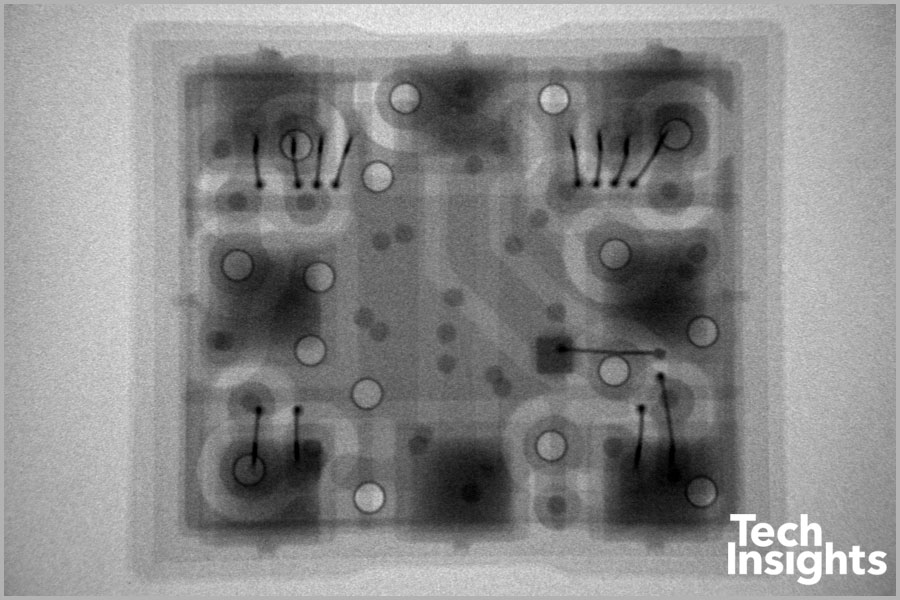
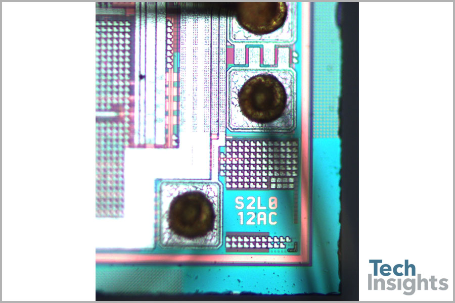
Last year we saw Apple use a front-facing ranging module (ToF chip + VCSEL) in the iPhone 7/7 Plus. We found the same chip, sourced from STMicroelectronics, re-used for the iPhone 8 Plus. The package dimensions are: 2.75 mm x 2.35 mm x 1.15 mm thick. The 1.17 mm x 1.97 mm ToF die has S2L012AC die markings.
Costing
We analyzed the 256GB iPhone 8 Plus with the Intel LTE platform and developed a quick turn cost estimate of $367.50. We then compared this to the iPhone 7 Plus with the same memory size and Intel LTE platform (Apples to Apples so to speak) from our teardown in January 2017. At $367.50, the iPhone 8 Plus was $33.00 more expensive to build than its predecessor.
- The bulk of the increased cost ($26.50) is due to the market price of DRAM and Flash memory components, which have increased significantly since January
- There is a $4.50 increase in the cost of the A11 over the A10
- There is another $3.50 worth of improvements in the cameras
- Costs drop $2.00 in the display due to reuse from the iPhone 7
- Costs in other categories go up and down a little due to a newer Intel LTE platform and other items, but they even themselves out in the end
[1] Sony To Use FD-SOI in Stacked Image Sensors
[2] Tim Cook: Augmented Reality is as big of a technology as the smartphone


