Discover the Google Pixel Watch's cutting-edge technology with our in-depth forecast and teardown analysis. Explore its design, components, and performance in this comprehensive TechInsights eBook.
Happy Holidays to all and to all a good cycle G. Dan Hutcheson The Chip Insider® IBM and Rapidus Partner to compete in the next World Cup of Semiconductors: 2nm foundry technology. The timing of this announcement was perfectly fitting for the holidays, because in a way it was IBM’s Christmas gift to
The outlook is gloomy as we head into 2023 Shereen Vaux Order activity for semiconductor equipment continued to decline, falling to 52 degrees The November data from the Taiwanese manufacturers was mixed TSMC continues to increase sales to record levels; this will likely worsen the excess
Join TechInsights’ Power Subject Matter Expert, Dr. Stephen Russell and Strategy Analytics’ Executive Director of the Powertrain, Body, Safety & Chassis (PBCS) and Electric Vehicles Service (EVS), Asif Anwar, as they present the Recent PMIC Innovation and an Automotive Market Outlook Power webinar.
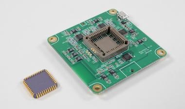
The BeyonSense Short Wave Infra-Red (SWIR) Sensor is part of a new generation of image sensors that capture light beyond the visible spectrum enabling imaging and sensing devices to see beyond the visible spectrum and into the internal structure of an object.
SEMI ISS Europe 2023 to Spotlight European Chips Act with Focus on Growth, Talent, Sustainability and Supply Chain VIENNA, Austria — December 13, 2022 — Leading analysts, economists, policymakers and technologists will gather at the SEMI Industry Strategy Symposium Europe (ISS Europe) 2023, February