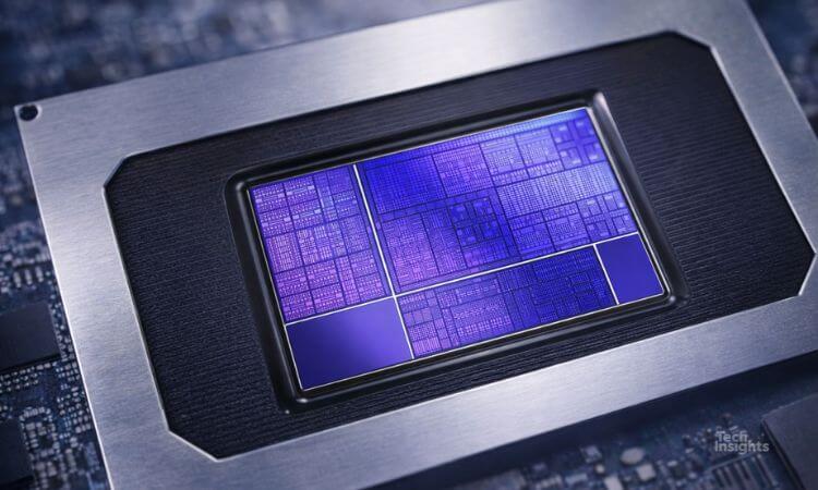
This report contains the following detailed information:
- Package photographs, top metal, and polysilicon die photographs
- SEM cross-sectional micrographs through the bit line (BL) showing the general structure of the DRAM cell array, die dielectric materials, and major features
- Shematic drawing of DRAM cell circuit diagram
- SEM bevel through the memory array showing memory array plan-view features and realignment of the image set between the active, WL, BL, and capacitor
- Memory cell layout analysis


