Disruptive Event
YMTC’s Xtacking 3.0, first to 200+ layers
This Chinese company is now the leader in 3D NAND Flash
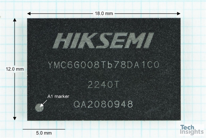
In early November 2022, TechInsights thought we had found YMTC’s Xtacking 3.0 inside the TiPlus7100. Now, in later November, we can confirm we have found Xtacking 3.0 inside the HikSemi CC700 2 TB SSD and this is the first 200+ layer 3D NAND Flash solution on the market, putting YMTC ahead of Samsung, Micron, Sk hynix, and other leaders.

How China’s YMTC leap-frogged Micron, Samsung
In 2016, Yangtze Memory Technology Corp. was born. YMTC was China’s response to the world’s insatiable demand for more and more digital storage, and a cornerstone for China’s mandate to have leading-edge, domestic chip manufacturing capabilities. (Note: China had initially kicked off a specific R&D program around storage 2014 – the foundation for what was to become YMTC.)
“Flash” memory is the primary digital storage technology today. It started as an extension of the relatively low capacity, non-volatile memory called EEPROM, or Electrically Erasable Programmable Read Only Memory. In the early days, it was used to store a small amount of code needed to start up or boot microelectronics systems.
Today, it has largely displaced hard disk drives for bulk data storage in high performance systems such as the phones, tablets, laptops, and PCs we use every day. And it has become essential for large-scale, enterprise and cloud-based storage.
In 2016 when YMTC got its start, the market leaders at the time were just transitioning to “3D” Flash – in other words, multiple layers of storage cells on a single chip. Samsung, Micron/Intel, Sandisk/Toshiba and SK Hynix were starting to get reasonable production yields in this new technology. Up until then, Flash chips were single layer. To get higher density, you stacked multiple chips into the same package. It took years for the market leaders to develop industrialize 3D Flash production. But when they did, memory densities suddenly increased by an order of magnitude or more. YMTC jumped over the fundamental single layer flash and hit the world stage with a 32-layer product.
As YMTC came in late to the game, there was plenty of skepticism that they could possibly compete on the world stage. Literally starting from scratch – YMTC broke ground on their first fab decades after the market leaders developed foundational Flash technology.
In 2018 – just two years after their start - YMTC announced their 64-layer technology. And in 2020, we saw it in full production. The market leaders at the time were already up to 90+ layers, but it was clear that YMTC was absolutely in the race – effectively just one generation behind.
Fast forward to November, 2022. TechInsights have just found YMTC’s 232 layer Flash. And although the (now former) market leaders are all working at the 200+ layer generation, YTMC is the first we’ve seen in production.
What does this mean?
If we used the past as our guide, YMTC would be the uncontested Flash technology leader before 2030. However, it will be almost impossible for YMTC to continue the pace. R&D costs at the leading edge aren’t linear – as technology progresses, R&D costs go up by many multiples to get to the next generation. On its own, YMTC isn’t generating enough revenue to support the ever-increasing costs of development. Although it wouldn’t come as any surprise to see public funds continuing to support YMTC’s development programs, US (really, world-wide) sanctions on advanced semiconductor manufacturing equipment will significantly hamper quick progress.
What YMTC has accomplished has been nothing short of amazing. Not only have they leap-frogged the biggest semiconductor companies in the world, but they did also it despite being headquartered in Wuhan, often facing crippling lockdowns during a worldwide pandemic. So, although the chips might seem to be stacked against them given today’s geo-political challenges, they certainly shouldn’t be ruled out.
Find content like this and more in the TechInsights Platform. Sign-up for free today.


