The 10nm Process Rollout Continues to Evolve

Explore the latest advancements in 10nm semiconductor technology, including Samsung's 10nm LPE and TSMC's 10nm FinFET processes. Learn about their impact on mobile devices like the Galaxy S8 and iPad Pro2, and discover how these innovations are driving the semiconductor industry forward.
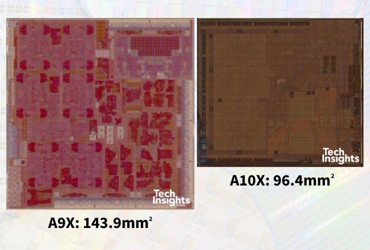
We expected the Samsung 10 nm LPE process, TSMC 10 FF process, and Intel’s 10 nm process in production this year. Samsung’s came in first with the release of the Samsung Galaxy S8, containing either a Samsung or Qualcomm designed APU, built on Samsung’s 10 nm LPE process. The march continues with the Apple A10X, which is confirmed to be built on TSMC’s 10 FF process. The A10X die size comes in at 96.4 mm2 as compared to the previous generation, A9X at 143.9 mm2, which was built on TSMC’s 16 FF-Turbo technology. This is an impressive full node scale, when accounting for the extra CPU cores built into the A10X and extra IP blocks of the A10 vs. A9 family. We estimate a 45% die level scale (0.55x the area of running on the previous technology), based on our detailed floorplan analyses of the Apple A-series.

A9X vs A10x (Dimensions to scale)
The Apple A10X was extracted out of the new iPad Pro2, available as of June 12. The original rumored release was slated for March 2017, and would have align to TSMC’s “Night Hawk” program’s stated goal to accelerate 10 FF R&D, in order to beat Samsung 10LPE’s known launch date of April 2017. The 1Q delay, along with well-known design losses of MediaTek’s Helio X30, also designed on TSMC 10 FF, shows a slower than anticipated ramp for this technology. This, along with TSMC’s statements that 10FF will be a short-lived technology to be quickly supplanted by 7 FF in 2018, indicates some non-ideal perf/power, area, and cost factors for this technology. We have launched in-depth analyses at the functional block floorplan level, standard cell library, process, as well as measuring the actual transistor performance.

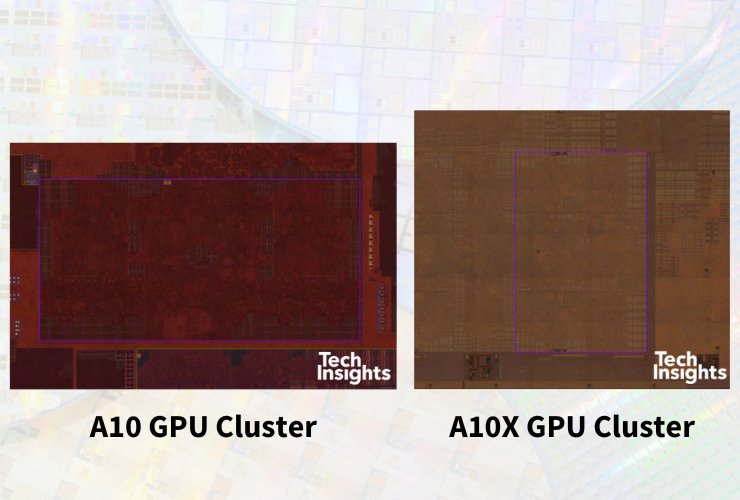
A10 vs A10x GPU Clusters (Dimensions to scale)
At an IP-block level, we can compare the GPU between A10 and A10X, which appear to be the same Apple customized Imagination PowerVR cores, which comes out ~49% area scale (0.51x the area of running on the previous technology). Again, this is an impressive full node scale, in the age of marketing naming confusion of what a technology node actually is. Unfortunately, the naming confusion will only continue going forward. Samsung 10 LPE scale factor vs. Samsung 14 LPP, for example, was only 36% at the IP block level, and node names have been announced down to “4 LPP”. Intel, on the other hand, has announced their 10 nm to be “hyperscaled” compared to their 14 nm, which according to their metric would lead to ~63% IP block level area scaling. Adding to the confusion, 10nm will likely be a long-lived node for both Samsung and Intel, and a short-lived node for TSMC, with multiple “7 nm” technologies around the corner, and a slew of other node names and node variants in between. The marketing battle is fierce for the hearts and minds of companies locked in fierce battles to dominate high margin mobile, data center infrastructure, and looking to win in the race to 5G, automotive automation, and pervasive artificial intelligence.


