EXCLUSIVE REVERSE ENGINEERING INSIGHTS
How Qorvo's 3D RF-SOI architecture is redefining smartphone RF front-end design
TechInsights reverse engineering reveals how hybrid bonding enables a new generation of compact, high-performance RF front-end devices.
Complete the form below to access the full Qorvo QM18566 analysis on the TechInsights Platform.
You'll also get access to the latest teardowns, market analysis, reverse engineering reports, and semiconductor intelligence covering the technologies shaping the consumer electronics industry.
Corporate email required. By submitting this form, you consent and agree to the creation of a TechInsights Platform account and agree to the terms of the End User License Agreement and Privacy Policy.
As smartphones continue adding more 5G bands, carrier aggregation combinations, MIMO antenna paths, Wi-Fi, satellite connectivity, and future wireless technologies, RF front-end components face a growing challenge: delivering more functionality without consuming more space.
Traditional planar RF-SOI architectures are approaching practical scaling limits. As RF switch networks become larger and more complex, increasing die size is no longer the most efficient path forward.
That's where TechInsights comes in.
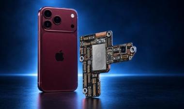
Our latest reverse engineering analysis of the Qorvo QM18566 RF Antenna Tuner, extracted from the Apple iPhone 17 Pro, reveals how Qorvo and UMC are leveraging 3D RF-SOI hybrid bonding to rethink RF integration. By distributing the RF switch network across two vertically bonded RF-SOI dies, the architecture delivers comparable switching capability in a substantially smaller footprint, creating a scalable foundation for future RF front-end designs.
Unlike its predecessor, the planar Qorvo QM18502 used in the iPhone 16 Pro, the QM18566 is fabricated using UMC's 55 nm 3DIC RF-SOI platform.
Instead of expanding a single die to accommodate increasingly complex RF switch networks, the QM18566 partitions those networks across two active RF-SOI dies connected through a dense Direct Bond Interface (DBI).
The result is an architectural shift rather than a simple process improvement—one that demonstrates how advanced packaging can unlock new scaling opportunities for RF front-end devices.
Hybrid bonding has become a major innovation for processors and high-bandwidth memory, but its adoption in RF front-end devices represents an important new direction for the semiconductor industry.
As foundries such as UMC and GlobalFoundries invest in 3D RF-SOI technologies, vertically integrated RF architectures are poised to become a key enabler for future antenna tuners, RF switches, and low-noise amplifiers.
Understanding these implementation strategies is becoming increasingly important for semiconductor manufacturers, foundries, RF designers, and competitive intelligence teams evaluating next-generation wireless technologies.
Read the full analysis to see exactly how Qorvo's QM18566 is built, and get TechInsights' take on which foundry is behind it.
The TechInsights Platform delivers exclusive reverse engineering insights that reveal how this breakthrough was designed, manufactured, and implemented.
Reverse-engineered RF switch architecture
Understand how Qorvo implemented its next-generation RF switch network and distributed it across a 3D RF-SOI architecture.
Complete floorplan comparison between the QM18502 and QM18566
Compare the architectural evolution from a conventional planar design to a vertically integrated 3D implementation.
UMC 55 nm RF-SOI process characterization
Explore detailed process technology analysis, including transistor structures, metallization, and fabrication techniques.
Hybrid bonding and Direct Bond Interface (DBI) analysis
See how wafer-to-wafer hybrid bonding enables dense interconnects and a compact 3D RF architecture.
High-resolution SEM and TEM cross-sections
Examine device structures with detailed imaging that reveals process integration and manufacturing implementation.
Circuit reconstruction and process integration analysis
Gain insight into how the circuit was designed, fabricated, and optimized to achieve its performance goals.
Packaging and die-level implementation details
Discover how package design and die integration contribute to the device's size, functionality, and overall architecture.
Our analysis reveals not only what changed, but how Qorvo implemented a new 3D RF architecture, and why that approach could shape the next generation of RF front-end design.
Gain Deeper RF Front-End Intelligence
The transition to 3D RF-SOI architectures marks an important evolution in smartphone RF design. TechInsights provides the in-depth reverse engineering needed to understand how these innovations are implemented, and what they mean for future RF front-end development.