Posted: June 14, 2017
Contributing Authors: Jeongdong Choe, Senior Technical Fellow
Samsung has begun to mass-produce their first 10 nm-class DRAM products, and we’ve taken this opportunity to analyze and compare it to the previous generations of 25 nm and 20 nm DRAM products. During our analysis, we discovered the technology node is 18 nm which we believe is the smallest half pitch used to design active pattern.
The Samsung 18 nm 8 Gb DRAM die has a 0.189 Gb/mm2. Compared to their 20 nm 8 Gb die, memory density has increased by 32.8%, while the cell size (0.0026 µm2) is decreased by 21.2%. Figure 1 shows a comparison of DRAM die size and memory density from Samsung, SK hynix and Micron’s 30 nm-class, 20 nm-class and 10 nm-class DRAM products.
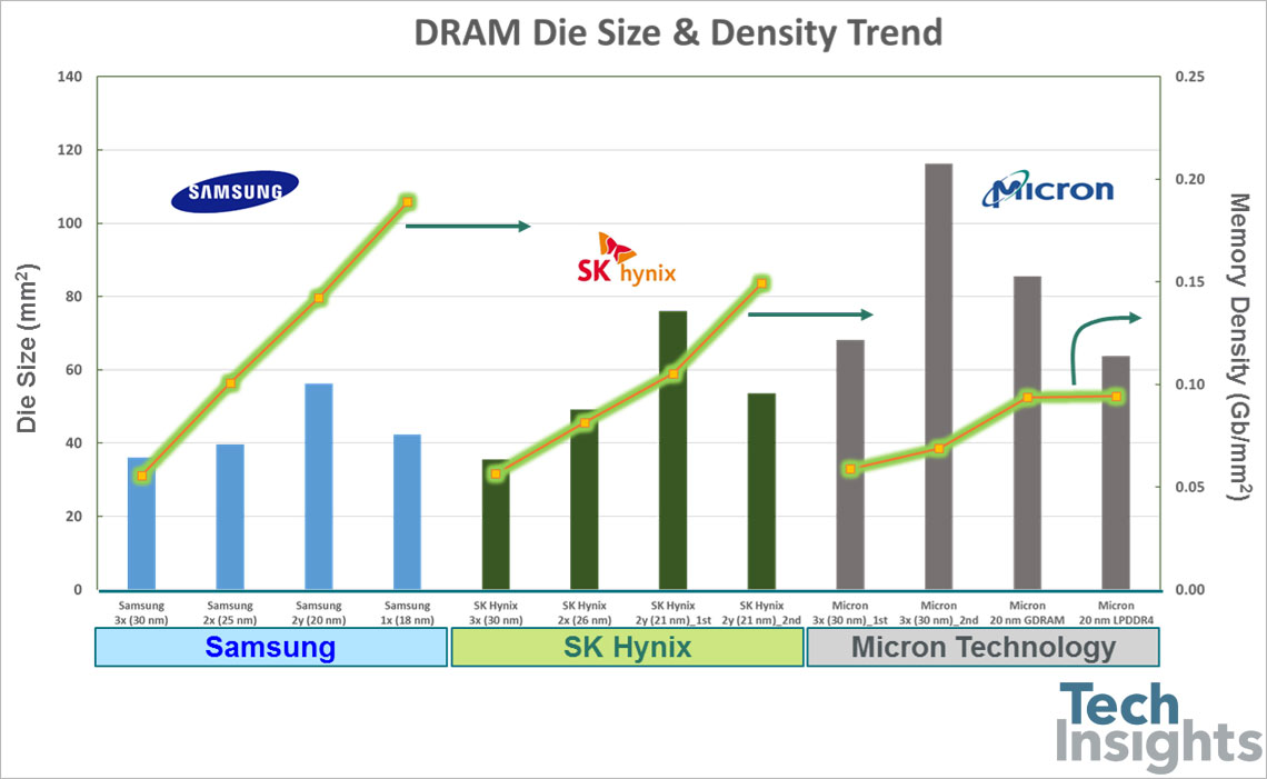
Figure 1. A comparison of DRAM die size and memory density from Samsung, SK Hynix and Micron.
We believe that one of the most innovative aspects of the Samsung 18 nm DRAM is a 10 nm-class patterning technology. For the first time, Samsung successfully developed and implemented a QPT (Quadruple Patterning Technology) on their 18 nm DRAM products including DDR4, LPDDR4 and LPDDR4X. A 48 nm wordline pitch and a 54 nm bitline pitch are used, while the active pitch is 36 nm, this means the active patterns are integrated by QPT. This technology has already been used for 1y nm NAND technology, especially for 15 nm (Toshiba/SanDisk) and 14 nm (Samsung) 2D planar NAND gate (CG/FG) patterning. DPT (Double Patterning Technology) has been used for 2D planar 1x and 1y nm NAND active and bitline patterning. Due to the matured QPT, Samsung may speed up the time to develop 1y nm (15 nm) DRAM for the next DDR5, LPDDR5 and GDDR6 products.
UPDATE! Samsung’s Anti-Fuse Technology found on 18 nm DRAM: Kilopass 2T-cell Technology used
For the honeycomb-type capacitor structure, ultra-thin and very uniform ZrO/AlZrO double layer high-k dielectrics have been used. With the previous technology for 20 nm-class DRAM, the dielectric layers were thicker at the top than the bottom, making the capacitors appear to be upside-down cones. Samsung developed a new material/process through the ultra-fine dielectric deposition technology, successfully making the thickness of the dielectric layer uniform to a few angstroms. This technical breakthrough allowed the birth of the first 10 nm-class DRAM with high performance and reliability. From our analysis on the Samsung 18 nm DRAM cell capacitor structure, 1.06 nm EOT (electrical oxide thickness), 1.77 MV/cm (ZrO) and 7.4 fF/cell capacitance can be extracted at 1.2V, 300K.
Download product information on Samsung 18nm DDR and LPDDR4X
Our product information includes: Samsung K3UH5H50MM-NGCJ (LPDDR4X Mobile SDRAM) and K4A8G085WC-BCRC (DDR4)