Apple M5 Pro Package Analysis: TSMC SoIC-X F2F Hybrid Bonding Enters Consumer Computing
Apple’s M-series Pro and Max processors have historically been defined by monolithic SoC integration. With the M5 Pro processor, Apple has taken a different architectural path.
TechInsights has completed a full package-level reverse engineering and process analysis of the Apple M5 Pro processor (APL1X15) extracted from the 14-inch MacBook Pro A3426. The analysis examines the disaggregated package architecture that separates CPU and GPU functions into chiplets connected through a silicon interposer. More significantly, the package uses TSMC’s SoIC-X face-to-face (F2F) chip-on-wafer (CoW) hybrid bonding technology, marking its first documented appearance in a consumer computing product.
This is not simply a packaging change. It is a structural shift in how Apple is balancing integration density, performance, manufacturability, and die-level economics in its high performance computing silicon.
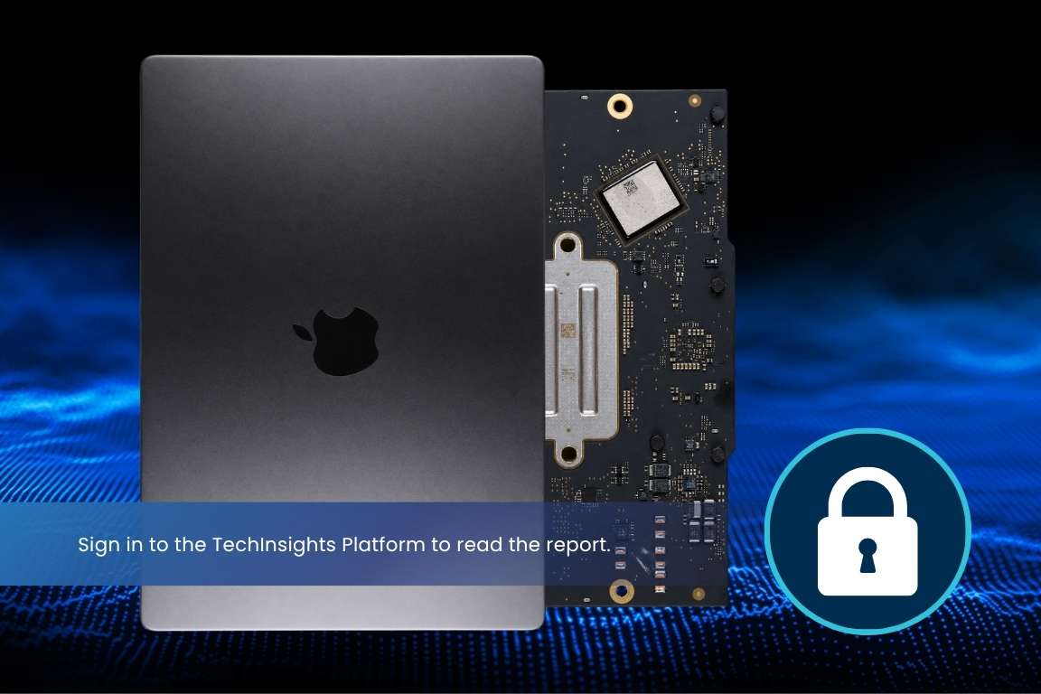
Figure 1 – TechInsights analyzes the Apple M5 Pro APL1X15 package, revealing TSMC SoIC-X F2F hybrid bonding, CPU and GPU chiplets, silicon interposer routing, and verified die costs. (Source: TechInsights)
How Apple Uses TSMC SoIC-X F2F Hybrid Bonding in the M5 Pro
TSMC SoIC-X has previously been documented in face-to-back (F2B) configurations, including memory-on-logic stacking in AMD’s V-Cache X3D gaming processors and Instinct AI accelerator families. In the M5 Pro, Apple is using SoIC-X differently.
The M5 Pro uses a face-to-face chip-on-wafer approach to assemble separate CPU and GPU chiplets onto a monolithic silicon interposer. Functionally, the package resembles a 2.5D integration architecture comparable to CoWoS-S, but with a critical difference: solder-based micro-bumps are replaced by bumpless hybrid bonding. That change has important electrical and architectural consequences. By moving to bumpless hybrid bonding, the M5 Pro can achieve substantially higher die-to-die interconnect density while reducing the parasitic losses that typically make chiplet-based designs less efficient than monolithic integration.
For product strategists, packaging engineers, and process technologists, this creates a new benchmark for evaluating advanced 2.5D integration. The M5 Pro is not only a case study in Apple’s silicon roadmap; it also provides physical evidence that SoIC-X F2F hybrid bonding is moving beyond previously documented AI accelerator and memory-on-logic implementations into consumer computing.
What the Reverse Engineering Analysis Reveals
TechInsights’ full package-level reverse engineering and process analysis examines the complete M5 Pro package architecture, including the CPU and GPU chiplets, silicon interposer, memory components, and die-level cost structure.
The analysis resolves several technical and strategic questions:
- What interconnect pitch and density TSMC has achieved in production with SoIC-X F2F chip-on-wafer hybrid bonding
- How the M5 Pro’s interposer routing compares with larger AI accelerator implementations
- What the full bill of materials shows across the processor package, chiplets, and memory
- What the verified die costs are for the CPU and GPU chiplets
- How Apple’s package architecture changes the comparison between monolithic and chiplet-based M-series designs
The evidence base includes cross-sectional SEM and TEM analyses, EELS compositional mapping, delayering, and dimensional metrology across all components of the package. These methods allow TechInsights to verify the structure, materials, interconnects, and integration choices behind the M5 Pro rather than relying on external specifications or product-level claims.
Create Your Account Today
The Apple M5 Pro analysis provides a detailed view of the package architecture, SoIC-X F2F hybrid bonding implementation, interposer routing, component bill of materials, and verified CPU and GPU die cost analysis.
*Some analyses may only be available with a paid subscription