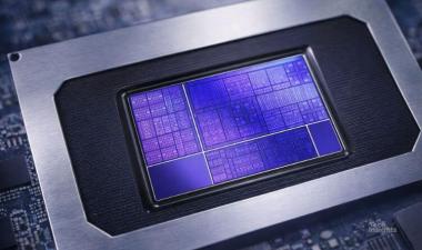
Meeting the Challenge: Advanced Packaging’s Role in Delivering Value
As the electronics industry moves towards more sophisticated applications, the challenges in packaging semiconductors present new opportunities.
Driven by the demand for smaller, high-functionality devices, Dick James highlights the shift from traditional transistor scaling, which followed Moore’s Law, to advanced packaging methods spurred by Design-Technology Co-Optimization (DTCO) since around 2000. This shift marks the second era of scaling, known as “More Moore,” characterized by innovations like 3D transistors.
Dan Hutcheson discusses the impact of economic factors, such as post-COVID inflation, on Moore's Law, noting that while the cost benefits are diminishing, the value of Moore's Law persists through chiplet technology. Chiplets, like those used in AMD's MI300 family, enable advanced performance scaling and power efficiency by integrating multiple chips within a single package. This approach is key to the third scaling era, termed 3D Power Scaling, which focuses on vertical device structures and heterogeneous integration.
In the first installment of our Advanced Packaging & Chiplets Summer Spotlight Series, we explore the emphasis that advancements in packaging technologies have had on chiplet design strategies, overcoming previous performance drawbacks. This development supports more-than-Moore technology integration, enhances yield through die size management, and fosters new business models in the semiconductor industry.
An advanced packaging solution tailored for your industry awaits. To read the full article and other content referenced, click here.


