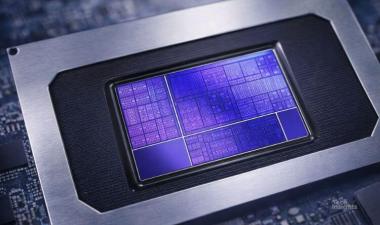
Samsung HBM3 from AMD Instinct MI300X HBM Interconnect and Packaging Analysis

Explore Samsung's HBM3 advanced packaging with 12Hi DRAM stacks, TSVs, and micro-bumps, powering AI and HPC with high bandwidth and efficiency.
This report provides deep insight into the advanced packaging innovations used in the manufacturing of Samsung's high bandwidth memory 3 (HBM3). It features a total of 12 DRAM dies (12Hi) vertically stacked and connected with through silicon vias (TSVs) and solder-based micro-bumps (µbumps). Reduced DRAM die thickness enables the increased number of stacked dies versus previously documented Samsung HBM2E. High bandwidth memory has been propelled to the forefront of high performance computing (HPC) by artificial intelligence (AI). AI models require vast amounts of training data, necessitating high capacity and high bandwidth memory access closely integrated with the processing cores. The 1024-bit bus of the JEDEC HBM standard and an integrated custom controller enables high data rates with relatively low clock speeds.


