What's inside the Google Pixel 6 Pro Teardown?
Contributing authors: Stacy Wegner, Daniel Yang, Radu Trandafir, Aakash Jani
The much anticipated Google Pixel 6 Pro has arrived in our lab for teardown. This one took us some time to find!
The phone used for the teardown is a Canadian model GA03161-CA, 128 GB that supports 5G Sub-6. Until very recently, rumors have been circulating that Google Pixel 6 series phones include many Samsung key silicon components. We are happy to put the rumors to rest: our quick teardown has confirmed it - there are a lot of Samsung components in key areas of this phone!
Google Pixel 6 Pro 128GB
| Google Tensor Application Processor PoP | |
| (Tensor AP + Micron 12 GB LPDDR5 MT62F1536M64D8CH-031 WT:A) | |
| Kioxia 128 GB NAND Flash Memory | |
| Samsung SHANNON A5123 5G Modem | |
| Samsung SHANNON 5511 RF Transceiver | |
| Maxim MAX77759A PMIC | |
| STMicroelectronics NFC Controller ST54K | |
| Maxim MAX20339EWB Surge protection IC | |
| NXP PCA9468 Battery Charger IC | |
| STMicroelectronics MCU ST33J2M0 | |
| Google H1D3M Titan M security processor | |
| Samsung Exynos SM 5800 Supply Modulator (2 pcs) | |
| Cirrus Logic CS35L41B Audio Amplifier (2 pcs) | |
| Cirrus Logic CS40L25 Audio Amplifier Haptic | |
| Broadcom BCM47765 GNSS Receiver IC |
| Skyworks SKY53737 FEM | |
| Skyworks SKY58260-11 FEM | |
| Samsung Exynos SM 5800 Supply Modulator | |
| Qorvo QM77080 FEM | |
| Skyworks SKY53738 FEM (3 pcs) | |
| Skyworks SKY77652-31 PAM | |
| Samsung Shannon 5311A PMIC | |
| IDT P9412 Wireless Charing Receiver IC | |
| Samsung PMIC S2MPG10 | |
| Samsung PMIC S2MPG11 | |
| Unknown, Wi-Fi/BT Module (likely) |
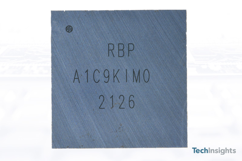
Google Tensor Application Processor
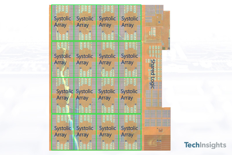
Google’s semi-custom application processor is all about AI. Google built a custom deep learning accelerator (DLA) to challenge Qualcomm and Samsung in inferencing. The custom DLA features 16 (4x4) instantiations of systolic arrays that outscore both Qualcomm and Samsung on ETH Zurich’s AI-Benchmark. While impressive, AI-Benchmark only tells half the story since it heavily relies on FP16 for inferencing. Most mobile AI network designers like to use INT8 for their layers because of the increased energy efficiency and comparable accuracy. For INT8 processing, the Pixel’s DLA lags both Qualcomm and Samsung in object detection, image segmentation, and image classification according to MLPerf 1.0.1 results.
TechInsights' lab team has done a great job in getting the Google Tensor processor die photos quickly.
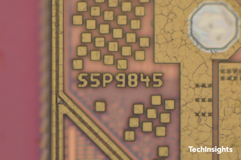
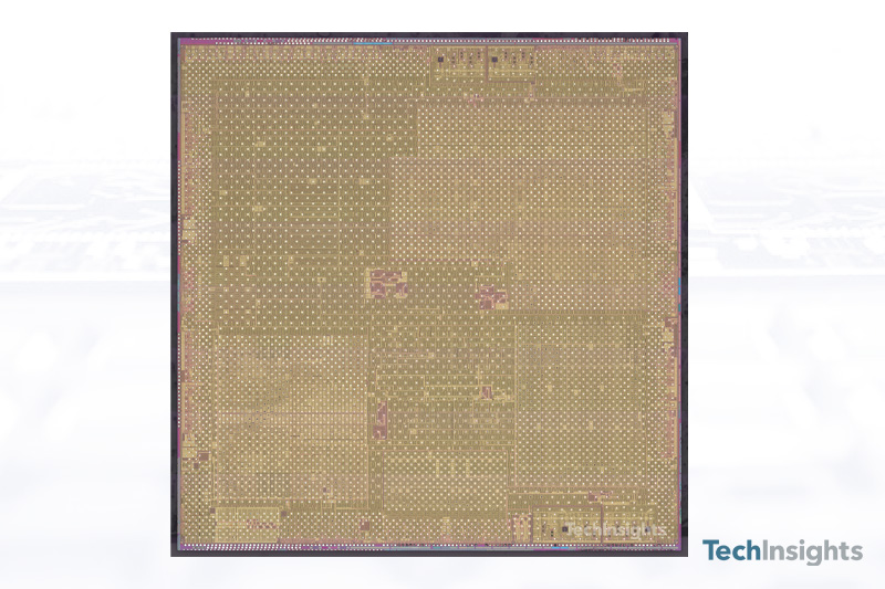
The Tensor die has a die size (seal) of 10.38mm x 10.43mm = 108.26mm2 and is fabbed on Samsung's 5nm process node technology. The following images show die marks and the die photo.
The die mark “S5P9845” conforms to the traditional Samsung Exynos processor naming rule, where the Exynos 990 Application Processor has the die marks of S5E9830, the Exynos 2100 5G SoC has die marks of S5E9840, and the Exynos 1080 5G SoC has S5E9815.
We have heard of possible ties between the Google Tensor and Samsung Exynos processors, and our analysis of the Tensor die continues. It does appear that the foundry supplier for the Tensor die is Samsung. We will confirm the process node soon, which we expect is in Samsung’s 5LPE.
Security
Google designed the Titan M2, which is a custom RISC-V controller, to support Android Strongbox, securely generating keys, storing passwords, and protecting PINs. The company tested and certified its Titan chip through an external evaluation lab, achieving AVA_VAN.5 certification—one of the highest levels for smartphones.
Mobile RF Components in the Google Pixel 6 Pro
On the mobile RF front, the Pixel 6 brings about some key new developments:
- Google / Samsung ties in the Tensor: Now that we have spent some time examining the Google Tensor SoC, we have analyzed the device tree file system of the Linux kernel for Google Pixel 6, and it shows that some blocks of the Google GS101 Tensor processor are shared with Samsung’s Exynos.
- A first for the US market: Samsung has developed a full 5G radio solution, which is included in the Pixel 6, making this the first major 5G phone in the US that does not include a Qualcomm modem.
Looking forward, we note that Oppo is looking to develop their own SoC solutions for higher end phones - is Qualcomm’s dominance in this space diminishing?
UWB Connectivity
Confirmed: the Google Pixel 6 Pro supports UWB connectivity, operating between 6489.6 MHz and 7987.2 MHz. Similar to the Galaxy S21 Ultra UWB design, the Google Pixel 6 Pro has multiple UWB patch antennas. However, in Google Pixel 6 Pro, only one antenna is used to transmit, whereas in the Galaxy S21 Ultra, two UWB antennas are used to send UWB signals.
Although the Google Pixel 6 Pro design has similar components to the Samsung Galaxy S20 and Galaxy S21 Ultra, the Teardown team identified a new Qorvo UWB component instead of the same NXP SR100T that was found in the Samsung Galaxy S21 Ultra.
WiFi 6E
Another point of similarity between the Google Pixel 6 Pro and the Samsung Galaxy S21 Ultra: the Pixel supports WiFi 6. This, however, is not just a protocol advancement - it requires new hardware designs. So far, we can confirm that the WiFi 6E modules from both phones include the Broadcom WiFi 6E SoC.
Samsung Design Wins
With the exception of the Google Tensor Application Processor - which is now in our , the phone's key components are from Samsung, including: Samsung SHANNON A5123 5G Modem, Samsung SHANNON 5511 RF Transceiver, SHANNON 5800 Envelope Tracker IC, Samsung SHANNON 5311A PMIC, And more!
The Samsung SHANNON A5123 5G Modem is not new to us. We originally found it in the Galaxy S20 Ultra in early 2020, where it paired with the Samsung Exynos 990 Application Processor as a standalone 5G Modem.
As we have confirmed that there is a standalone Samsung 5G Modem in the Pixel 6 Pro, it stands to reason that the Google Tensor is an Application Processor without integrated Modem functionality, but we have not seen the die photos yet - we will confirm when we do.
The Samsung SHANNON 5511 RF Transceiver is not new to us either. We originally found it in Samsung Exynos 1080 and 2100 5G SoC platform smartphones, such as Vivo X60 and Samsung Galaxy S21 series in early 2021.
Additional Design Wins
In Memory, the Google Pixel 6 Pro we have torn down has a Micron 12 GB LPDDR5 which should have 8 pieces die of Micron’s 1y nm 12 Gb LPDDR5.
KIOXIA has won the NAND Flash slot.
There is a standalone GNSS Receiver IC from Broadcom. The BCM47765 is the company’s second generation Dual-Frequency (L1+L5) GNSS chip. TechInsights has analyzed the first generation BCM47755.
The Pixel 6 Pro supports NFC and Wi-Fi/BT functions too. We have identified two likely modules and will confirm them through further analysis.
STMicroelectronics keeps the NFC slot design win with the same die that we have seen in the Google Pixel 4 and Pixel 4 XL. We have confirmed that inside the wireless combo IC module is the Broadcom BCM4389 Wi-Fi 6E and Bluetooth 5 wireless combo SoC, which we first saw in the Samsung Galaxy S21 Ultra 5G phone.
Google Pixel 6 Pro US Model GA03149-US
We have now done a quick tear down on a Google Pixel 6 Pro GA03149-US, a United States model of the phone that supports 5G mmWave and Sub-6.
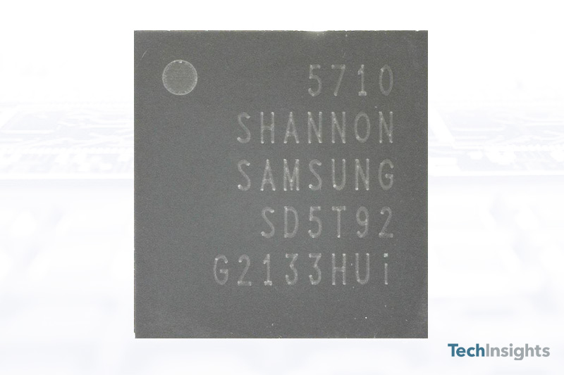
Comparison with the Canadian model we have been examining shows that the US model has a Samsung mmWave RF Transceiver Exynos RF 5710. So Samsung is the second silicon supplier of the 5G NR mmWave cellular chipsets, alongside Qualcomm. TechInsights will be creating a series of reverse engineering reports on the Exynos RF 5710 for our Mobile RF Analysis subscribers.
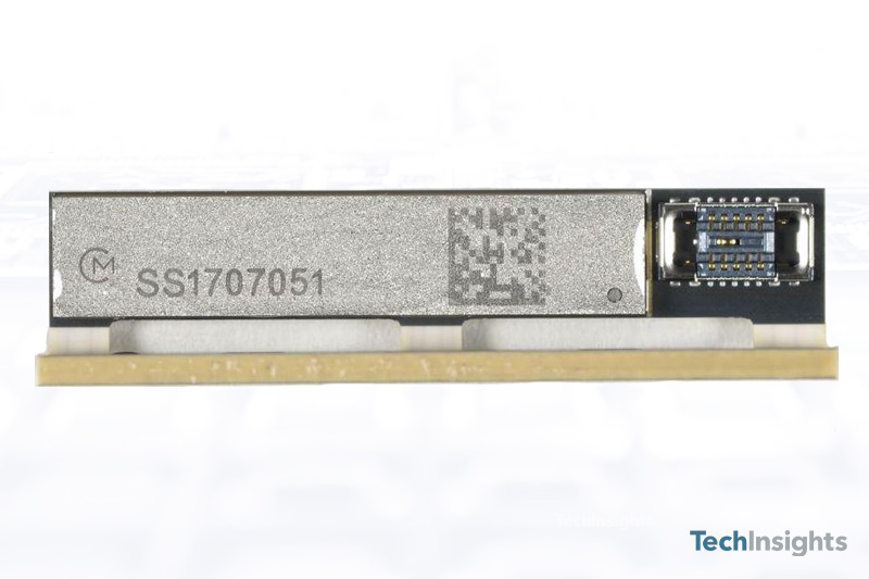
We have also found a Murata mmWave Module SS1707051 found in the US phone. We are currently working to identify the die inside.
Find content like this and more in the TechInsights Platform. Sign-up for free today.


