Monday, August 5, 2019 / 5:30pm to 10:00pm PST
Hyatt Regency (Cypress Room), 5101 Great America Parkway, Santa Clara
TechInsights’ Presentation and Networking Reception at Flash Memory Summit
TechInsights is hosting an exclusive networking event at the Hyatt Regency Hotel, Santa Clara. Please complete the form on this page no later than July 31st to reserve your spot.
Agenda
5:30 to 6:00pm - Sign-in
6:00 to 6:45pm - NAND Flash and SSD Evolution with Internal Probing and Waveform Analysis
Neil MacLeod, Systems Analyst
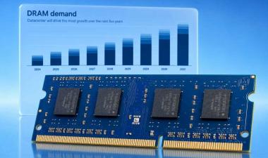
7:00 to 8:00pm - DRAM, NAND and Emerging Memory Technology Updates: Process, Design and 3D Architecture
Dr. Jeongdong Choe, Senior Technical Fellow at TechInsights
8:00 to 10:00pm - Networking Reception
This reception is open to local area professionals and attendees of Flash Memory Summit.
Detailed presentation abstracts, and the registration form for the event, are below.
August 5, 2019
5:30pm to 10:00pm PST
Duration 4 1/2 Hours
6:00 to 6:45pm - NAND Flash and SSD Evolution with Internal Probing and Waveform Analysis
Neil MacLeod, Systems Analyst
Many players have entered and grown in the SSD market, especially with the accelerated collection and use of data by large corporations and their data centers. Data centers are quickly ramping up their use of SSDs, and this has driven the SSD market to high competition in both price and performance. This, in turn, has driven innovation at the SSD system and component levels, particularly in the areas of controllers and NAND flash memory devices.
In a flash memory system, commands are sent by the controller to NAND flash memory devices. The device internally applies various voltage algorithms to the memory cells to perform the desired functions (e.g. read, program and erase). Using custom IC circuit reverse engineering and probing methods on various planar and 3D MLC and TLC NAND flash memory devices, we uncover and analyze the internal mechanisms that comprise the major operational functions.
The architecture and functionality have changed significantly with 3D NAND when compared to planar NAND, and in turn this has driven changes in waveform algorithms. Additionally, competition among memory manufacturers to achieve superior performance has driven innovation around more complex waveforms to achieve further precision on memory bit programming while minimizing durations. TechInsights’ internal NAND flash memory waveform analysis includes the capture of wordline, bitline and sourceline voltages of select memory cells for various operations, such as programming and reading a page of data and erasing a block, to uncover these innovations.
At the system level, the SSD, which consists of NAND flash memory devices and the controller, has changed significantly to accommodate both a growing number of pages per block from 3D NAND, and further enhancement of drive performance when storing at TLC or denser bits per cell. With the capture of the NAND flash traffic between the controller and a NAND flash package (ONFI and JEDEC NAND), we can uncover the innovations that drive the ability to use TLC storage and still achieve high performance, and we can identify the changes in addressing required to accommodate the increasing number of bits needed for page addressing in the limited address space.
7:00 to 8:00pm - DRAM, NAND and Emerging Memory Technology Updates: Process, Design and 3D Architecture
Dr. Jeongdong Choe, Senior Technical Fellow at TechInsights
Most of the major memory chip makers have been positioning themselves well on DRAM, NAND and Emerging Memory demands, although DRAM and NAND memory prices have been falling recently. 1x nm DRAM products including DDR4, LPDDR4X and GDDR6 are commercialized by Samsung, Micron and SK Hynix, and 1y nm DDR4 and LPDDR4X products have been revealed from Samsung and Micron. Some new technologies have already been adopted for 1x and 1y node, and more are coming on 1z and 1a (1α) or 1b (1β). Further DRAM cell scaling down will be discussed.
Currently 512 Gb NAND dies are very common with 64L/72L and 92L/96L 3D NAND and have been widely used for µSD, SSD and mobile devices. Intel/Micron and Samsung have revealed 1 Tb QLC NAND dies with their 64L 3D NAND structure. SK Hynix just announced their new 128L NAND products. Samsung has introduced Z-NAND (Z-SSD) 1st generation with 48L V-NAND SLC cell array. Small form factor BGA and UFS are also common for mobile devices. All the major NAND players are racing toward higher density 3D NAND integration, as if there are no limits on developing the next 3D NAND generation.
Intel extends XPoint memory application not only for conventional and DC SSD but also DCPMM, while Micron’s QuantX has been delayed. Everspin’s 3rd gen. STT-MRAM (pMTJ) and Adesto’s 2nd gen. CBRAM technologies are quite interesting. Emerging memory products are just jumping into the high-density memories with over 1 Gb/die. Do you think emerging memories can replace the high-density SRAM/DRAM cells soon? To continue to the next generation of memory devices, cell structure, materials, 3D architecture and its process integration should be changed. We’ll discuss together on what memory players are doing for current and future challenges. Don’t miss out.
Attendee takeaways include:
- An overview of recent and upcoming developments in DRAM and NAND technologies
- An understanding of the design approaches taken by key industry players Intel/Micron, Samsung, and SK Hynix
- An overview of emerging and exploratory memory products from Intel, Micron, Everspin, and Adesto
8:00 to 10:00pm - Networking Reception
This reception is open to local area professionals and attendees of Flash Memory Summit.
August 5, 2019
5:30pm to 10:00pm PST
Duration 4 1/2 Hours
Register to attend this event

Apple M5 Pro Package Analysis: TSMC's SoIC-X F2F Hybrid Bonding in Consumer Computing
TechInsights analyzes the Apple M5 Pro APL1X15 package, revealing TSMC SoIC-X F2F hybrid bonding, CPU and GPU chiplets, silicon interposer routing, and verified die costs.

Why the AI Memory Shortage Could Keep DRAM and NAND Prices High for Years
AI-driven demand is creating the biggest memory shortage in history. Discover why DRAM and NAND prices are expected to remain elevated through the rest of the decade.
DRAM Market Update Q2 2026: Why This Cycle Looks Different
Stronger-than-expected demand, rising AI memory requirements, evolving procurement models, and record profitability are transforming the DRAM market in ways that differ from those of previous cycles.
![]()
The Authoritative Information Platform to the Semiconductor Industry.

