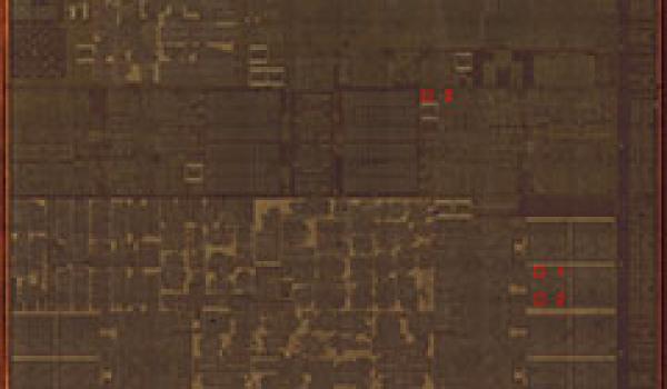
This project presents a Standard Cell Essentials Analysis of the Intel Cannon Lake i3-8121U DDR I/O region. It is a collection of scanning electron microscopy (SEM) montage images showing transition regions between an I/O IP block and a digital logic block, showcasing dummy structures and relationship to system-on-chip (SoC) design rules used on Intel Cannon Lake i3-8121U. The report includes:
- Downstream product features and system-on-chip (SoC) level areas of analysis
- Technology node contact and back end of line (BEOL) process architecture assessment with stack-up dimensions
- Features and dummy structures of the SoC design overhead associated with the transition between design IP blocks
- Scanning electron microscope (SEM) montage image of the analyzed bevel areas delivered in CircuitVision
- Target areas are typically transitions between different types of IP blocks, such as analog I/O to digital, or to memory, and typically contain many dummy features


