Critical process technology insights for patent owners & product development teams
Organizations with IP portfolios that include semiconductor process technology require solid technical data on competitors’ processes to understand best how to leverage their IP. For design groups, understanding the processes used by competitors gives insight into achieving size, cost, power or performance targets.
TechInsights’ state-of-the-art facilities, proprietary tools, products, and highly experienced technicians and engineers help clients to:
- Support IP campaigns with valuable evidence of use information on semiconductor technology
- Track key innovations used (critical dimensions and design rules, new materials, modified structures, etc.)
- Make informed decisions about IP and technology investments
Revealing the innovation others can't
TechInsights has invested extensively in developing tools, methods and technical know-how to understand today’s cutting edge packaging technologies.
Our technical package reverse engineering capabilities include:
- Package Planar Optical microscopy
- Package X-ray Imaging Package Cross-section
- SEM (Scanning Electron Microscopy) and Optical Microscopy Package Delayering
- Optical Microscopy and Trace back analysis Package material analysis
- SEM EDS (Energy-dispersive X-ray spectroscopy)
- Others
- TEM (Transmission Electron Microscopy) Imaging
- TEM EDS and EELS material analysis
- SMIM (Scanning Microwave Impedance Microscopy)
Breadth and depth of devices analyzed
TechInsights’ staff have investigated a wide range of devices and processes such as:
- Advanced CMOS processes from all major foundries
- DRAM and NAND flash memories including 3D/Vertical NAND
- BCD processes from a variety of manufacturers
- RF SOI processes
- Power transistors
- Image sensors
- MEMS
- Emerging memories
- Semiconductor packaging
- LEDs, solar cells and other optoelectronic devices
- Displays
- Lithium ion batteries
Staff skilled in the art
We have an experienced and knowledgeable staff, with industry background, which understands past current and upcoming semiconductor technology.
Our engineering staff is skilled in evaluation of large patent portfolios to identify the most valuable patents, matching them with appropriate devices and archived analysis, and providing evidence of use.
Major archive of semiconductor analysis & devices
Large inventory of semiconductor devices available for analysis, starting from the 1980s.
Unmatched library of off-the-shelf reports for IP or competitive technical intelligence use:
- Newest devices from major industry players, across all current process types and nodes
- Extensive prior art library with reports dating back to the 1980s, containing the combined archives of TechInsights and Chipworks
Responsive solutions tailored to your exact needs
TechInsights has over 30 years of experience working with top process technology patent holders to understand and leverage process patent value.
We have the IP expertise, industry experience, capacity, and reverse engineering facilities to support your patent and technology teams.
Our analysis:
- Is always customized to your specific needs to ensure maximum return on your investment
- Goes as deep as required to discover and explain the nature of an innovation or prove patent value

Apple A20 Pro: Inside the iPhone 18 Pro’s TSMC 2nm Processor
TechInsights analyzes Apple’s A20 Pro processor, revealing TSMC N2 gate-all-around technology, expanded AI and graphics processing, and a new side-by-side memory packaging architecture.

iPhone 18 Pro Max Unboxing and First Look
Watch TechInsights unbox the Apple iPhone 18 Pro Max before our experts begin detailed teardown and semiconductor analysis.
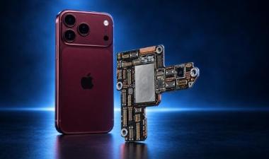
Apple iPhone 18 Pro Max Teardown: A20 Pro, X80 and Apple N1
See what TechInsights’ preliminary teardown reveals about the iPhone 18 Pro Max, including its A20 Pro processor, Qualcomm X80 modem, Apple N1, and new mmWave hardware.

The Authoritative Information Platform to the Semiconductor Industry.