Hybrid Bonding –Tomorrow’s Interconnect
A Detailed Look at Hybrid Bonding’s Role in Advanced Semiconductor Packaging
March 10, 2025 On-Demand Webinar
How is hybrid bonding revolutionizing semiconductor packaging with high-density 3D copper-to-copper connections for next-gen HPC and near-memory computing?
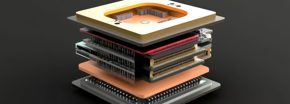
How hybrid bonding is evolving to enable advanced interconnect scaling
Technical examples from image sensors, NAND, HBM, and 3D integration
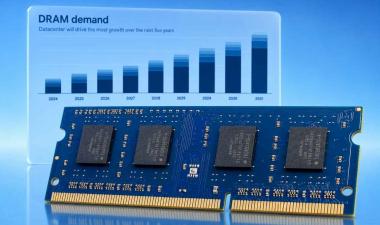
Key market drivers and the growing ecosystem behind adoption