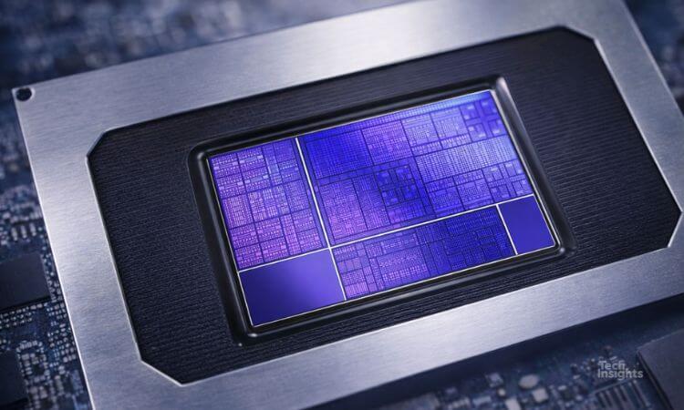
The Advanced CMOS Essentials (ACE) deliverable for Advanced Packing comprises a concise analyst’s summary document highlighting observed critical dimensions and salient features supported by the following image folders:
- Downstream product teardown
- Package photographs and X-rays
- Top metal die photographs
- Optical cross section of general package structure
- SEM cross section of the general package structure, metals, dielectric materials, die and package interconnect
- SEM cross section of TSV, where applicable
- Optical and SEM bevel images of the package assembly


