YMTC's Memory Developments Highlight China's Strong Position
YTMC’s latest Xtacking4.0 process has been observed in a new memory chip from the Chinese vendor. What can it tell us about the development of the domestic Chinese semiconductor industry in the face of US sanctions?

1 Step Forward, 70 Layers Back
YMTC hit the headlines last year with the 232 Layer TLC 3D NAND device, which was the most dense memory ever produced, not just in China but globally. YMTC is clearly a company to watch in the memory space. That was using the company’s Xtacking3.0 process. Now TechInsights has found YMTC’s Xtacking4.0 process in a commercial product, the ZhiTai TiPlus7100 Black Myth SSD.
The bit density is very advanced, 512 Gb on a tiny 40.44 mm2 sealed die size, which means a 12.66 Gb/mm2 die bit density. Although it’s not the most dense memory available, it’s competitive with the top devices. This is achieved through the hybrid wafer bonding structure and the newly designed 20 vertical channel holes.
The increase in the vertical channels is the key improvement in this iteration of Xtacking, an area where YMTC has a technology lead over the competition. It’s notable that YMTC were the first to introduce backside source connect (BSSC) in Xtacking3.0, and they remain the only memory company with a commercial product using this technology.
Although this next generation of process marks a step forward, it’s also notable that the number of layers is reduced significantly, with 70 fewer than the previous generation. Other memory providers have also reached the 232-layer yardstick. Why the step(s) back?
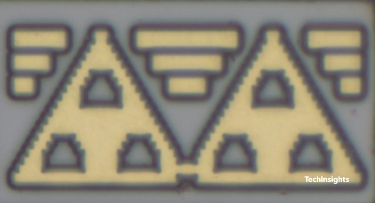
Misty Mountain Hop
The markings on the die are a double circumflex, “^^”. This type of die logo, without die labels, first appeared in the Huawei Pura 70 Ultra. There are rumors of the "Wudang Shan" (Mount Wudang) project, the transition of YMTC to utilize domestic supplies and tools. It is tempting to interpret these die marks as double mountain peaks, indicating that this device is part of the drive to domestic tools. This device therefore provides a yardstick for China’s own initiatives to create a domestic semiconductor ecosystem in the face of US sanctions, which have been particularly focused on tools.
Unusually for the industry, YMTC did not reveal the number of layers in the device specifications; so unusual in fact that it seems like a deliberate obfuscation. However, TechInsights was able to uncover this information through a combination of process and system analysis. We believe that the lower complexity and die sizes are to deal with lower yield issues from a relatively immature Chinese equipment ecosystem. This provides further evidence that this device is indeed manufactured using at least some domestic equipment.
The Big Picture
China’s “Made in China 2025” plan had the goal of making China the world’s leader in semiconductors along with building a vertical supply chain. They had set aside billions to do it. Conversely, the US is increasing sanctions on chipmaking tools and other technology to China.
This YMTC device shows that China is at the cutting edge when it comes to memory. Find out more about the technology and the political moves influencing it by reading the full report.