Unlock the Future of Advanced Packaging: A Deep Dive into Hybrid Bonding
April 14, 2025 3 Min Read
Hybrid Bonding is Reshaping the Semiconductor Industry. Are You Ready?

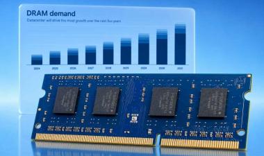
As the demand for higher performance, greater integration, and lower power consumption intensifies, traditional interconnect solutions are hitting their limits. Hybrid bonding has emerged as a critical enabler of next-generation semiconductor packaging—powering breakthroughs in high-performance computing (HPC), storage, and AI applications.
What You’ll Learn:
- Technology Fundamentals – Discover what makes hybrid bonding different—and why it’s vital for scaling interconnects.
- Ecosystem Readiness & Manufacturing - Get a closer look at the evolving infrastructure: materials, equipment, and processes enabling adoption.
- Key Application Segments – Understand hybrid bonding’s role across logic, memory, and image sensors.
- Adoption Barriers & Challenges - Explore the technical and ecosystem hurdles still facing industry players.
- Market Outlook – Access expert insights and forecasts for hybrid bonding’s adoption trajectory.
Since first spotlighting hybrid bonding in 2016, TechInsights has tracked its rapid evolution—and today, the technology is at a tipping point. Foundries, IDMs, OSATs, and equipment suppliers are making bold investments. This eBook offers the strategic insights you need to stay ahead.
A Deep Dive into Hybrid Bonding - Read the eBook for free
TechInsights delivers an in-depth look at the current state and future potential of hybrid bonding technology, based on nearly a decade of reverse engineering and market intelligence.
Unlock the Future of Advanced Packaging
Stay ahead of the curve and gain a competitive edge with exclusive insights into the technology that's transforming chip design and advanced packaging.