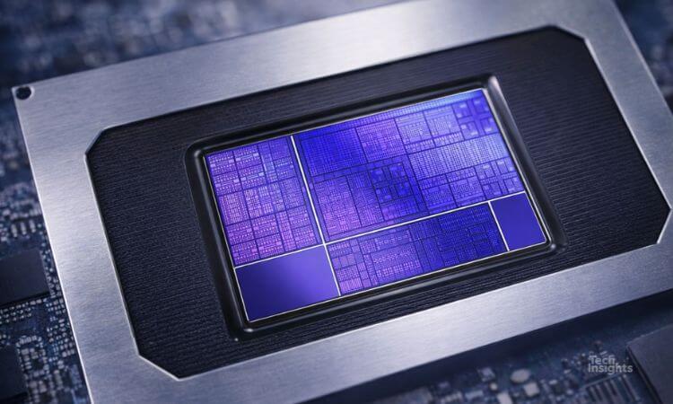
This is an Advanced CMOS Essentials (ACE) Summary document of the Micron MT43A4G40200NFA-S15 ES:A Hybrid Memory Cube Gen 2 (HMC2) 3D package analysis. Concise analyst’s summary of critical device metrics, scanning electron microscopy based energy dispersive X-ray spectroscopy (SEM-EDS) of package materials, and salient features supported by the following images:
- Package photographs and X-rays
- Die photographs
- Optical Bevel images and printed wiring board (PWB)
- SEM and optical cross section of the general package structure, metals, dielectric materials, die, through silicon vias(TSVs) and package interconnect structure


