
Assembly and Test Cost and Price Model
In-depth cost and price model for advanced package types including multi-die applications.
This model caters to a diverse spectrum of clientele, spanning from Integrated Device Manufacturers (IDMs) and fabless semiconductor companies to analysts, consultants, electronic systems firms, automotive enterprises, and beyond.

To understand this evolving landscape, you need a strong industry-leading business analysis tool.





Market Analysis Solutions




End Market Analysis:





The Semiconductor Manufacturing Economics Advantage
These products give any organization unique and detailed insights into the semiconductor supply chain. Customers include the world’s largest IDMs, foundries, fabless, electronics systems, automotive companies, equipment OEMs and materials suppliers, analysts, universities, and start-ups.
Supported Assembly Processes:
Leadframe, organic substrate (such as BGA, PGA, and LGA), ceramic substrate, wafer level, and InFO, including multichip and chiplet packages.
Supported Wafer Size:
75mm, 100mm, 125mm, 150mm, 200mm, and 300mm.
Supported Cost Elements:
Overall wafer sort, assembly and final test cost, assembly and tests processes, plus material usage.

Apple iPhone 18 Memory Costs: DRAM & NAND Price Pressure
DRAM and NAND prices are rising through the iPhone 18 launch. See what higher memory costs could mean for Apple, AI, BOM costs, and smartphone strategy.

Apple iPhone 18 Pro: A20 Pro, Camera, C2 Modem & Key Changes
Explore what is new in the Apple iPhone 18 Pro and Pro Max, including the 2 nm A20 Pro, variable-aperture camera, C2 modem, cooling, and battery.
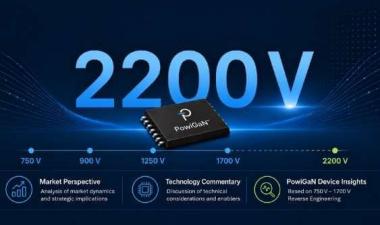
Can 2200 V PowiGaN Challenge Silicon Carbide?
Access TechInsights’ special report on Power Integrations’ 2200 V PowiGaN demonstration and its potential impact on high-voltage power semiconductor markets.

The Authoritative Information Platform to the Semiconductor Industry.