![]()
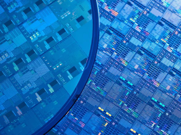
IC Cost and Price Model
End-to-end cost and price model for low-power silicon integrated circuits.
Presenting a self-contained and comprehensive solution model that finds its utility in various applications, including benchmarking, price evaluation, and market research. This versatile tool is not only suited for Purchasing Departments but also extends its benefits to Integrated Device Manufacturers (IDMs), fabless companies, analysts, consultants, electronics systems entities, automotive companies, and a host of other industries.
To understand this evolving landscape, you need a strong industry-leading business analysis tool.


Market Analysis Solutions
End Market Analysis:
The Semiconductor Manufacturing Economics Advantage
These products give any organization unique and detailed insights into the semiconductor supply chain. Customers include the world’s largest IDMs, foundries, fabless, electronics systems, automotive companies, equipment OEMs and materials suppliers, analysts, universities, and start-ups.
Supported Assembly Processes:
Over 700 processes by company (in production only), and process node covering established products in ASIC, CIS, DSP, MCU, Mixed Signal, RF, DRAM, Flash, and Embedded Memory applications. (No advanced DRAM, and no 3D NAND – Strategic Model only).
Supported Wafer Size:
100mm, 125mm, 150mm, 200mm, and 300mm.
Supported Cost Elements:
Wafer cost, wafer test, packaging, and final test on 8 (eight) entries.

Apple M5 Pro Package Analysis: TSMC's SoIC-X F2F Hybrid Bonding in Consumer Computing
TechInsights analyzes the Apple M5 Pro APL1X15 package, revealing TSMC SoIC-X F2F hybrid bonding, CPU and GPU chiplets, silicon interposer routing, and verified die costs.

Why the AI Memory Shortage Could Keep DRAM and NAND Prices High for Years
AI-driven demand is creating the biggest memory shortage in history. Discover why DRAM and NAND prices are expected to remain elevated through the rest of the decade.
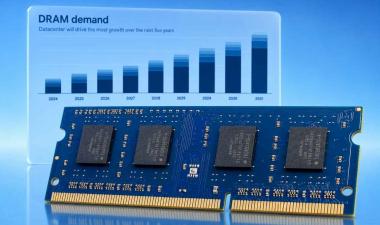
DRAM Market Update Q2 2026: Why This Cycle Looks Different
Stronger-than-expected demand, rising AI memory requirements, evolving procurement models, and record profitability are transforming the DRAM market in ways that differ from those of previous cycles.
![]()
The Authoritative Information Platform to the Semiconductor Industry.

