![]()
Semiconductor Packaging
Detailed analysis profiling cutting-edge packaging innovations seen in real-world products from industry leaders.
Combines technology, reverse engineering, analytics, related news, and our packaging industry roadmap to provide the analysis you need to navigate the semiconductor packaging market.
To read highlights of our experts' Advanced Packaging analyses, click here.

Whether you are a product manufacturer, OSAT, IDM, foundry, or fabless semiconductor company, packaging technologies impact your technical decisions and designs.
The Semiconductor Packaging Advantage
Integrated circuits are at the heart of modern technology and are continually evolving, becoming smaller, faster, and more energy-efficient, while expected to operate reliably in a range of conditions on Earth and in space. Packaging technologies are critical as they protect the IC from impact, heat, light, contamination, and even radiation but are also instrumental in enabling size reduction, managing heat, and improving performance. Packaging technologies continue to evolve to improve one or more of the following areas.
- Performance improvements through better die-to-die or chip-to-chip interconnect
- Size/volume reduction enabled by higher levels of integration
- Reliability improvements including:
- Protection from contamination, heat, and radiation
- Mechanical stability through cycling conditions
- Fewer defects/greater yield
- Manufacturing/integration cost reduction
Packaging Technology Innovation
The benefits seen in advanced packaging are typically driven by technical innovation in one of the following areas:
These comprise innovations at the package architecture level which simplify the integration of heterogeneous devices into a single package. Example technologies include:
- System in package (SiP)
- Multi-chip module (MCM)
- Antenna in package(AIP)
- Chiplets
- Discrete components in redistribution layer (RDL)
- CMOS image sensor, image sensor processor, filter, and lens stack with actuation
- Underfill materials to reduce mechanical stress
- Encapsulation to protect the die from environmental contamination
- Epoxy and thermal paste improve heat distribution
- EMI shielding
- Hybrid bonding including wafer-to-wafer (W2W), face-to-face (F2F), chip-to-wafer (C2W), face-to-back (F2B)
- Flip chip, Through-silicon via (TSV)
- Interposer/bridges/high-density (HD) routing
- Fan-in and fan-out wafer-level packaging (FI-WLP, FO-WLP)
This is increasingly important as devices become more complex, power-hungry, and utilize stacking options that impact the device’s thermal profile. Innovation areas include:
- Thermal interface materials (TIMs)
- Microfluidics (future)
- System-level considerations
Semiconductor Packaging Subscription
The TechInsights Semiconductor Packaging subscription provides access to upcoming and back-catalog reports that analyze packaging innovation found in leading real-world products in the areas of advanced logic, memory, RF, power, and image sensors. The reports are combined with images, data analytics, expert commentary, industry news, and technology briefings in the TechInsights Platform, creating a comprehensive landscape of the packaging domain.
The Semiconductor Packaging Subscription delivers insights across the following four key technology segments:
Growth in big data, AI, and multifunction portable devices are driving the need for high-performance, compact, and energy-efficient processing solutions, all of which are only achievable with advanced packaging technologies.
The Logic and Memory Packaging subscription is focused on packaging technologies found in advanced ICs and innovative memory devices including processors, application processors, GPUs, ASICs, DDR, NAND, and more.
The analysis covers source product information and images, optical die and package imaging, X-rays, and SEM cross-section analysis of the package structures and materials including metals, dielectrics, and interconnect along with SEM planar and isometric view of the package assembly.
RF system performance and energy efficiency is a critical factor of 5G handsets that significantly influences customer experience. Packaging is very tightly coupled to the overall RFIC design.
The Radio Frequency IC Packaging analysis profiles system co-design of front-end components such as LPAMiD and L-PAMiF, XCVRs, Rx Diversity, antenna in package, and mm-Wave TxRx front-end modules from the latest cutting-edge 5G handsets from leaders and disruptors such as Apple, Google, Samsung, Xiaomi, Oppo, Motorola, and more.
The analysis covers source product information and images, optical die and package imaging, X-rays, and SEM cross-section analysis of the package structures and materials including metals, dielectrics, and interconnect along with optical planar-view images of selected PWB metal layers.
The power semiconductor market is experiencing strong growth driven by several key factors including the trend towards vehicle electrification, the need for better power conversion efficiency in data center and renewable energy systems, and the quest for longer battery life in portable electronics. The introduction of wide bandgap semiconductors and advanced packaging technologies has brought about significant improvements in power device performance.
Power Semiconductor Packaging analysis profiles package level structural and materials innovation on Si, SiC, GaN, and power management ICs, Intelligent Power Modules, IGBT, Si MOSFETs, and more.
The analysis covers source product information and images, optical die and package imaging, X-rays, and SEM cross-section analysis of the package structures and materials including shielding, substrate, and interconnect.
The image sensor market is going through phenomenal innovation driven by a range of high-growth application areas including automotive, mobile, security, biometrics, and industrial/machine vision.
The Imager and Optical Sensor Packaging analysis profiles structural, materials, and key feature analysis targeting the most innovative and disruptive imager and optical/3D sensing technologies including camera modules, time-of-flight (ToF), optical in-display fingerprint sensing, ambient light sensors, and more.
The analysis covers source product information and images, module/package photographs and X-rays, module/package cross-sections, SEM-EDS of select features, die photograph, and phase detection autofocus (PDAF) classification. Key details of the camera module and package assembly are shown including:
- Shielding structures (metal, plastic, etc.)
- Lens mount strategy
- Lenses (number, type), spacers
- IR filter, glass window, etc.
- Substrate (type, metals, vias, etc.)
- Autofocus actuator
Advanced Packaging Analytics
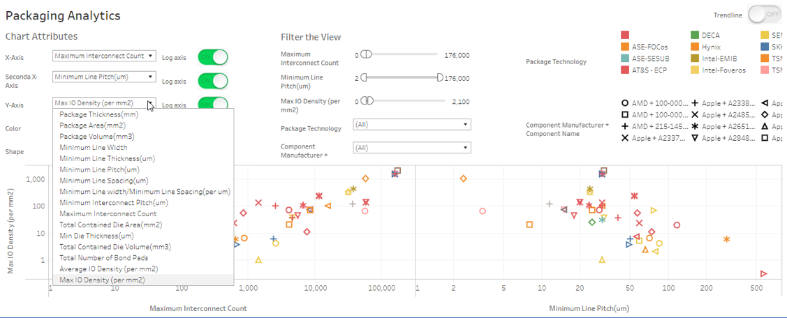
The Logic and Memory Packaging segments also include advanced Logic and Memory Packaging analytics which delivers charting capabilities to visualize the evolution of Logic and Memory packaging technologies deployed over time from leading component manufacturers. Users can select the metrics of interest, customize chart settings, and immediately see the results.
This foundational dataset spans multiple chip generations and enables users to deliver real-time visualizations of developing trends and correlations to help you answer critical questions such as how does the I/O density of packaging technology scale as interconnect counts increase? (Correlation between I/O density and interconnect count)
Learn more about the valuable insights revealed by the analytics in the TechInsights Platform.
Related Market Analysis on Semiconductor Packaging
In addition to detailed technical analysis, TechInsights also provides a range of market analyses covering key technology areas. The following is a list of related market analyses targeting Semiconductor Packaging and are available from the TechInsights Chip Market Research Service (CMRS) and Semiconductor Manufacturing Economics.
- Advanced Packaging Equipment History and Forecast 2017-2028
- Quarterly and Yearly Assembly and Packaging Equipment Forecast
- Worldwide Regional Assembly Equipment Consumption
- Assembly and Packaging Market Share
Semiconductor Manufacturing Economics
- Assembly and Test Cost and Price Model
- See how the Packaging+ Carbon Module lets users swiftly calculate the cradle-to-gate carbon impact of an IC product, providing IC designers, IDMs, and manufacturers with the data needed to make informed decisions on product designs and product carbon footprints.

Apple M5 Pro Package Analysis: TSMC's SoIC-X F2F Hybrid Bonding in Consumer Computing
TechInsights analyzes the Apple M5 Pro APL1X15 package, revealing TSMC SoIC-X F2F hybrid bonding, CPU and GPU chiplets, silicon interposer routing, and verified die costs.

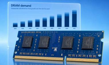
Why the AI Memory Shortage Could Keep DRAM and NAND Prices High for Years
AI-driven demand is creating the biggest memory shortage in history. Discover why DRAM and NAND prices are expected to remain elevated through the rest of the decade.
DRAM Market Update Q2 2026: Why This Cycle Looks Different
Stronger-than-expected demand, rising AI memory requirements, evolving procurement models, and record profitability are transforming the DRAM market in ways that differ from those of previous cycles.
![]()
The Authoritative Information Platform to the Semiconductor Industry.

